IPC-SM-782A 表面安装设计和焊盘设计标准(带BGA).pdf - 第38页
tolerances should be discussed with the board manufac- turer .) The tolerances are based on copper thickness up to and including one ounce copper . For each ounce of addi- tional copper , an additional 0.03 mm [0.001 in]…
Spacing requirements are usually the inverse of the toler-
ances shown for conductors in Table 3–9. For additional
information see IPC-D-310, Artwork Generation and Mea-
surement Techniques.
3.6.4.2 Conductor Width and Spacing Tolerances
The
presentation in Table 3–9 represents process tolerances that
can be expected with normal processing. (Specific process
IPC-782-3-23
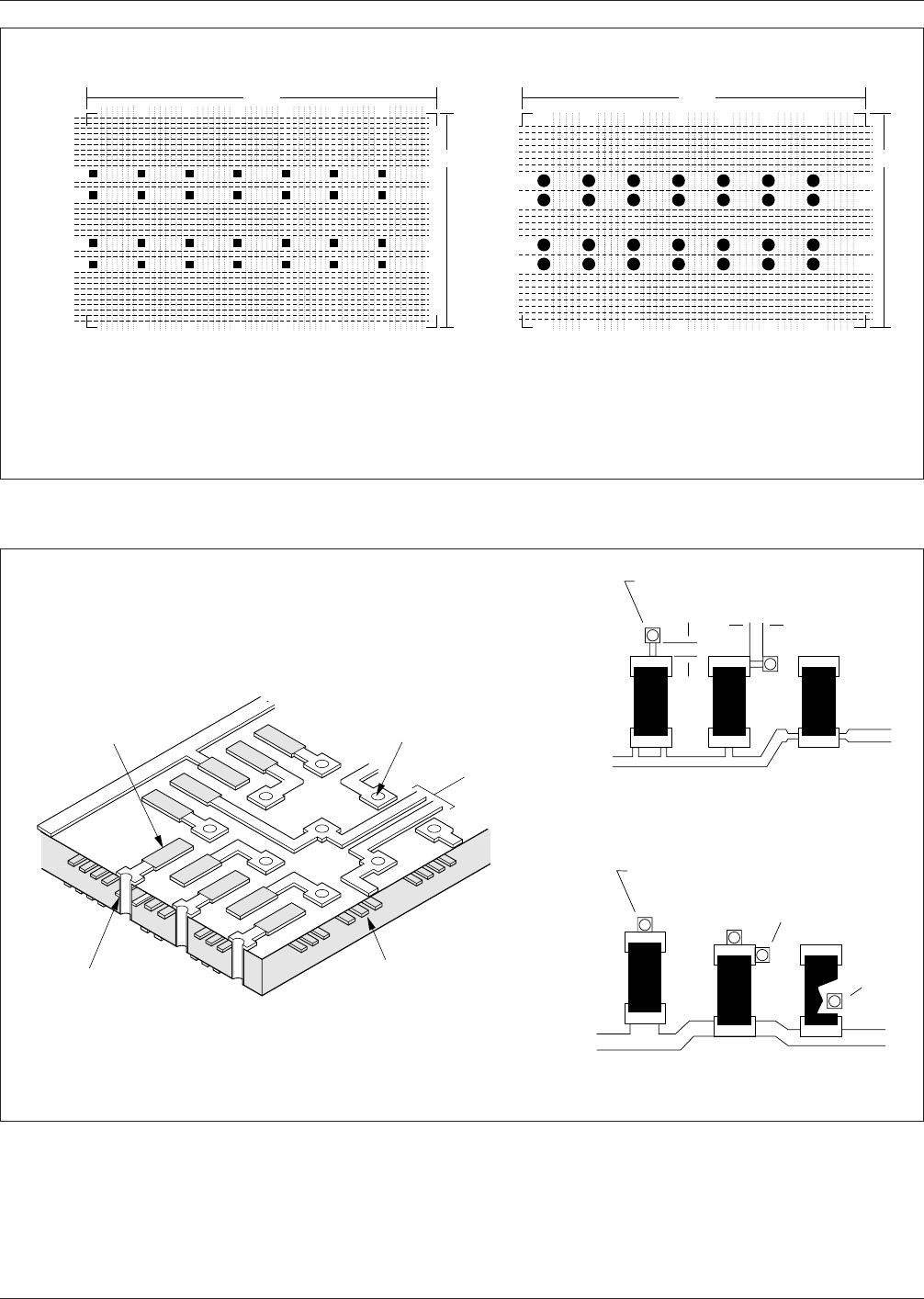
Figure 3–23 Routing channels under SOIC land pattern with 28 pins
49 Routing Channels
0.6mm Square lands
0.25mm Routing Grid
0.125mm Conductors/Clearances
32
Routing
Channels
35 Routing Channels
23
Routing
Channels
▼
▼
16mm
10mm
▼
▼
▼
▼
15mm
9.5mm
▼
▼
0.8mm Round lands
0.3mm Routing Grid
0.15mm Conductors/Clearances
IPC-782-3-24
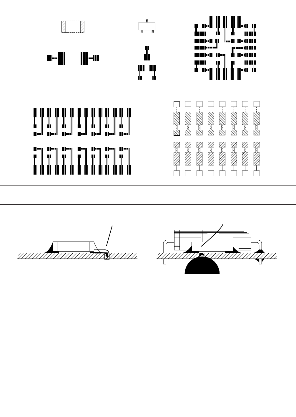
Figure 3–24 Land pattern to via relationships
Typical land
Inside layer connection
0.5 mm [0.020 inch]
diameter
Two 0.2 mm [0.008]
wide Conductors
Three 0.15 mm [0.006 inch]
wide Conductors between holes
▼
▼
▼
▼
▼
Square land
0.50mm
[0.020] min
Chip Components and Feed Through Via Holes
0.50mm
[0.020] min
Good Design
Poor Design
Feed through lands flush against contact area
▼
▼
▼
Too close
to contact
area
December 1999 IPC-SM-782A
29
电子技术应用 www.ChinaAET.com
tolerances should be discussed with the board manufac-
turer.) The tolerances are based on copper thickness up to
and including one ounce copper. For each ounce of addi-
tional copper, an additional 0.03 mm [0.001 in] variation
per conductor edge can be expected.
3.6.4.3 Conductive Pattern Feature Location Tolerance
The presentation in Table 3–10 is for the tolerance to be
applied to the nominal dimension chosen for the location of
the lands, connector contacts and conductors in relation
tothe datums. This tolerance includes tolerances for master
pattern accuracy, material movement, layer registration and
fixturing.
3.6.4.4 Annular Ring Control
The annular ring is
defined as the amount of land that is remaining after a hole
is drilled through it. With high density SMT designs, main-
taining minimum annular requirements has emerged as one
of the most difficult parts of multilayer PB fabrication in
terms of producibility. Perfect registration will maximize
the annular ring all around the drilled hole. Using a 0.8 mm
[0.030 in] land with a 0.5 mm [0.020 in] drill will result in
a 0.15 mm [0.006 in] annular ring under perfect registra-
tion conditions. If misregistration of 0.15 mm [0.006 in]
occurs in any direction, the result will be a 0.3 mm [0.010
in] annular ring on one side of the pad, and no annular ring
on the other side. If misregistration is greater than 0.15 mm
[0.006 in], i.e., 0.2 mm [0.008 in], then the drill will actu-
ally break out of the land. If the breakout is in the direc-
tion where the conductor connects to the land, the drill will
effectively disconnect the conductor from the land. The net
IPC-782-3-25
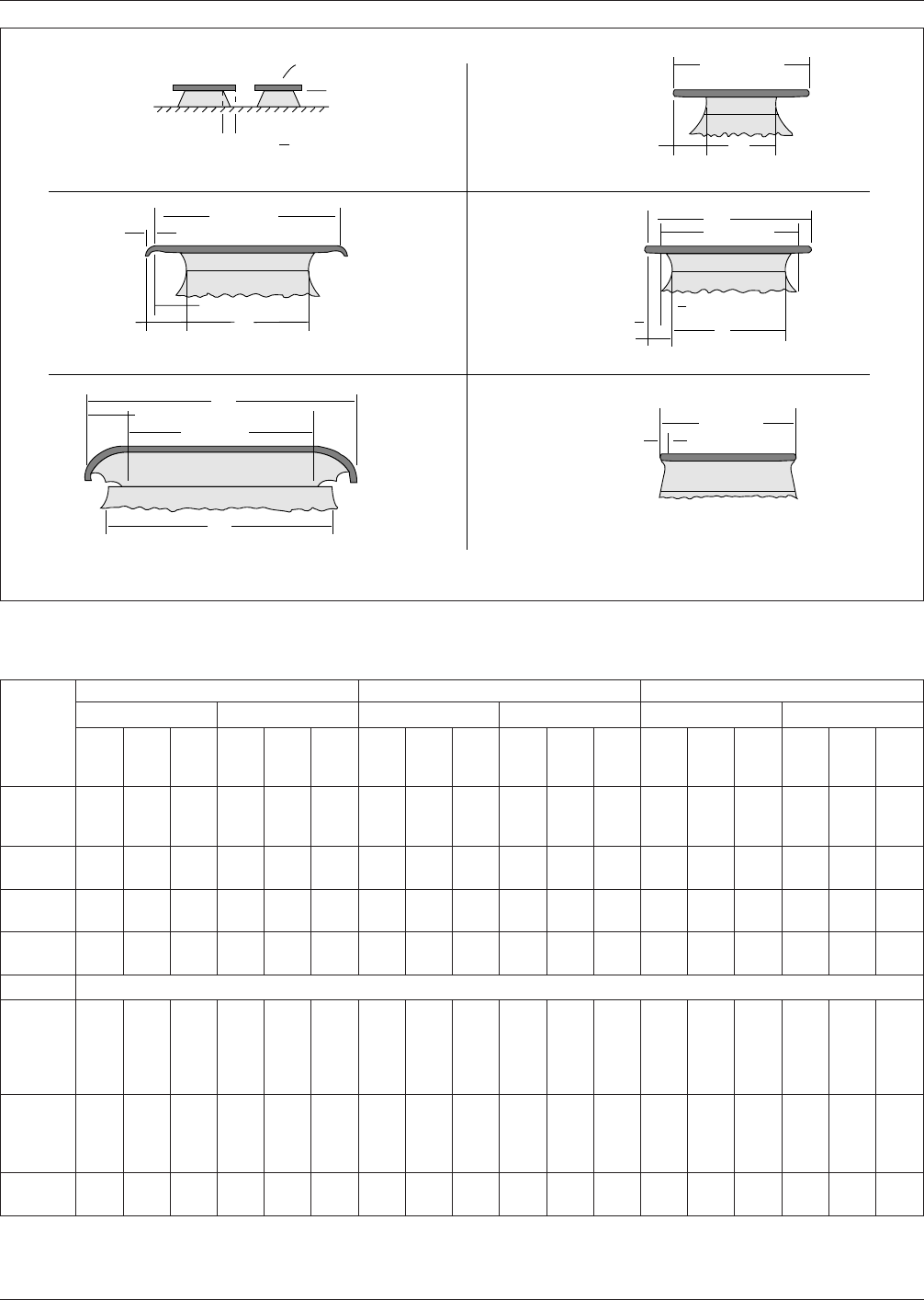
Figure 3–25 Examples of via positioning concepts
Side 2
Vias
Side 1
Vias
Side 1
Vias
Side 2
Vias
Chip component
Chip component
PLCC
SOIC
SOIC
IPC-782-3-26
Figure 3–26 Vias under components
Caution
Solder
Characteristic
Solder
Migration
▼
▼
Wave Solder
▼
IPC-SM-782A December 1999
30
电子技术应用 www.ChinaAET.com
IPC-782-3-27
Figure 3–27 Conductor characteristics
▼
LaminateX
▼
Etch Factor =
V
X
An etch factor of 1/1 is usually considered practical.
Higher factors may be specified for some applications.
Resist
▼
V
▼
▼
"B" (DCW)
"E" Outgrowth
▼
▼
▼
▼
▼
▼
▼
"C" Undercut
▼
"A"
(MCW)*
Overhang
Panel Plating (Liquid Resist)
▼
▼
(OCW)*
▼
▼
"D"
"B" (DCW)*
"E" Outgrowth
▼
▼
(MCW)*
"A"
▼
▼
Pattern Plating (Liquid Resist)
▼
"B" (DCW)
(MCW)*
"C" Undercut
& Overhang
Panel Plating (Dry Film Resist)
▼
▼
"A"
▼
▼
▼
▼
▼
"D"
▼
"A"
(MCW)*
Overhang
Pattern Plating (Dry Film Resist)
▼
▼
▼
(OCW)*
"B" (DCW)*
▼
▼
▼
▼
"E" Outgrowth
▼
▼
"C" Undercut
▼
▼
"B" (DCW)*
▼
"C" Undercut
▼
Thin Clad & Pattern Plating (Dry Film Resist)
A = MCW (Minimum Conductor Width) B = DCW (Desi
g
n Conductor Width) D = OCW (Overall Conductor Width
Table 3–8 Typical Values to Be Added or Subtracted to Nominal Production to Achieve Desired Nominal Conductor Width
Description
1/2 Oz. Copper 1 Oz. Copper 2 Oz.Copper
Panel Pattern Panel Pattern Panel Pattern
Screen
Liquid
Photo
Dry
Film
Photo Screen
Liquid
Photo
Dry
Film
Photo Screen
Liquid
Photo
Dry
Film
Photo Screen
Liquid
Photo
Dry
Film
Photo Screen
Liquid
Photo
Dry
Film
Photo Screen
Liquid
Photo
Dry
Film
Photo
Subtractive
Method
Simple Etch
+25µm
[+0.0010]
+25µm
[+0.0010]
+25µm
[+0.0010]
— — — +38µ
[+0.0015]
+38µm
[+0.0015]
+38µm
[+0.0015]
— — — +63µm
[+0.0025]
+63µm
[+0.0025]
+63µm
[+0.0025]
———
Bare Copper
[PTH]
+38µ
[+0.0015]
+38µm
[+0.0015]
+50µm
[+0.0020]
-25µ
[-0.0010]
-25µm
[-0.0010]
-25µm
[-0.0010]
+50µm
[+0.0020]
+50µm
[+0.0020]
+63µm
[+00025]
0 0 +50µm
[+0.0020]
+76µm
[+0.0030]
+76µm
[+0.0030]
+89µm
[+0.0035]
+38µm
[+0.0015]
+38µm
[+0.0015]
+89µm
[+0.0035]
Tin-Lead
[PTH]
+38µm
[+0.0015]
+38µm
[+0.0015]
+50µm
[+0.0020]
-25µm
[-0.0010]
-25µm
[-0.0010]
+25µm
[+0.0010]
+50µm
[+0.0020]
+50µm
[+0.0020]
+63µm
[+0.0025]
0 0 +50µm
[+0.0020]
+76µm
[+0.0030]
+76µm
[+0.0030]
+89µm
[+0.0035]
+38µm
[+0.0015]
+38µm
[+0.0015]
+89µm
[+0.0035]
Gold Nickel
[PTH]
+38µm
[+0.0015]
+38µm
[+0.0015]
+50µm
]+0.0020]
-25µm
[-0.0010]
-25µm
[-0.0010]
+25µm
[+0.0010]
+50µm
[+0.0020]
+50µm
[+0.0020]
+63µm
[+0.0025]
0 0 +50µm
[+0.0020]
+76µm
[+0.0030]
+76µm
[+0.0030]
+89µm
[+0.0035]
+38µm
[+0.0015]
+38µm
[+0.0015]
+89µm
[+0.0015]
For Deposited Copper Thickness Equivalents
Additive
Method
Electroless
Copper
No-Etch
— — — -50µ
[-0.0020]
-25µm
[-0.0010]
-0µm
[0.0000]
— — — -76µm
[-0.0030]
-50µ
[-0.0020]
-0µ
[-0.0000]
— — — -101µ
[-0.0040]
-76µm
[-0.0030]
-0µm
[-0.0000]
Semi Additive
Method
Copper-No
Overplate
— — — -50µm
[-0.0020]
-25µm
[-0.0010]
-0µm
[-0.0000]
— — — -76µm
[-0.0030]
-50µm
[-0.0020]
-0µm
[-0.0000]
— — — -101µm
[-0.0040]
-76µm
[-0.0030]
-0µm
[-0.0000]
Tin Lead
Overplate
— — — -76µm
[-0.0030]
-50µm
[-0.0020]
-25µm
[-0.0010]
— — — -101µ
[-0.0040]
-76µm
[-0.0030]
-25µm
[-0.0010]
— — — -127µm
[-0.0050]
-101µm
[-0.0040]
-25µm
[-0.0010]
December 1999 IPC-SM-782A
31
电子技术应用 www.ChinaAET.com