IPC-SM-782A 表面安装设计和焊盘设计标准(带BGA).pdf - 第114页
6.0 TOLERANCE AND SOLDER JOINT ANALYSIS Figure 4 provides an analysis of tolerance assumptions and resultant solder joints based on the land pattern dimensions shown in Figure 3. Tolerances for the component dimensions, …
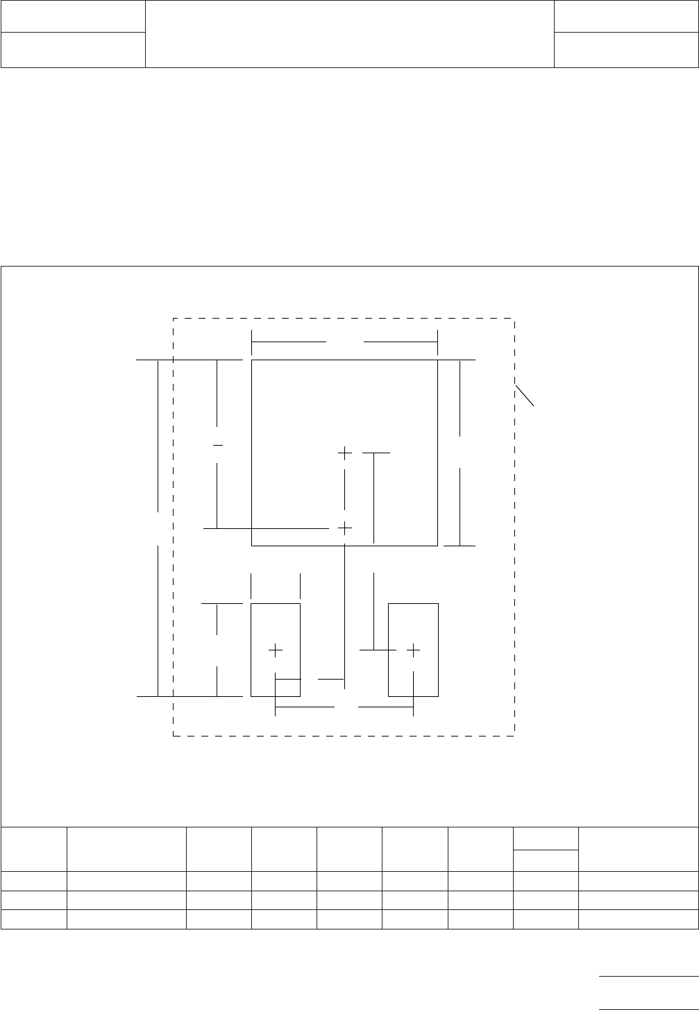
5.0 LAND PATTERN DIMENSIONS
Figure 3 provides the land pattern dimensions for TO 252
components. These numbers represent industry consensus
on the best dimensions based on empirical knowledge of fab-
ricated land patterns.
In the table, the dimensions shown are at maximum material
condition (MMC). The least material condition (LMC) should
not exceed the fabrication (F) allowance shown on page 4.
The LMC and the MMC provide the limits for each dimension.
The dotted line in Figure 3 shows the grid placement court-
yard which is the area required to place land patterns and
their respective components in adjacent proximity without
interference or shorting. Numbers in the table represent the
number of grid elements (each element is 0.5 by 0.5 mm) in
accordance with the international grid detailed in IEC publica-
tion 97.
RLP No.
Component
Identifier Z (mm) Y1 (mm) Y2 (mm) X1 (mm) X2 (mm)
C (mm)
Placement Grid
(No. of Grid
Elements)
ref
235A TS-003* 11.20 1.60 6.20 1.00 5.40 7.30 24x16
236 TS-005** 16.60 3.40 9.60 1.00 6.80 10.10 36x24
237 TO 268 19.80 3.40 13.40 1.40 13.60 11.40 42x34
Figure 3 TO 252 land pattern dimensions
▼
▼
▼
▼
▼
▼
▼
▼
X2
C
Y1
Z
▼
▼
▼
Grid
placement
courtyard
▼
▼
X1
E1
Dimensions are in millimeters
E2
▼
▼
▼
▼
Y2
▼
▼
Z
2
IPC-782-8-11-3
IPC-SM-782
Subject
TO 252/TO 268
Date
5/96
Section
8.11
Revision
A
Page3of4
电子技术应用 www.ChinaAET.com
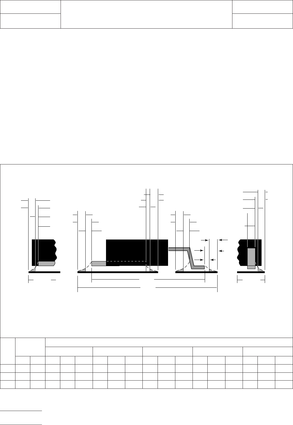
6.0 TOLERANCE AND SOLDER JOINT ANALYSIS
Figure 4 provides an analysis of tolerance assumptions and
resultant solder joints based on the land pattern dimensions
shown in Figure 3. Tolerances for the component dimensions,
the land pattern dimensions (fabrication tolerances on the
interconnecting substrate), and the component placement
equipment accuracy are all taken into consideration.
Figure 4 provides the solder joint minimums for toe, heel, and
side fillets, as discussed in Section 3.3. The tolerances are
addressed in a statistical mode, and assume even distribution
of the tolerances for component, fabrication, and placement
accuracy.
Individual tolerances for fabrication (‘‘F’’) and component
placement equipment accuracy (‘‘P’’) are assumed to be as
given in the table. These numbers may be modified based on
user equipment capability or fabrication criteria. Component
tolerance ranges (C
L
,C
S
, and C
W
) are derived by subtracting
minimum from maximum dimensions given in Figure 2. The
user may also modify these numbers, based on experience
with their suppliers. Modification of tolerances may result in
alternate land patterns (patterns with dimensions other than
the IPC registered land pattern dimensions).
The dimensions for minimum solder fillets at the toe, heel, or
side (J
T
,J
H
,J
S
) have been determined based on industry
empirical knowledge and reliability testing. Solder joint
strength is greatly determined by solder volume. An observ-
able solder fillet is necessary for evidence of proper wetting.
Thus, the values in the table usually provide for a positive sol-
der fillet. Nevertheless, the user may increase or decrease the
minimum value based on process capability.
RLP
No.
Tolerance
Assumptions
(mm)
Solder Joint
Toe (mm) Heel 1 (mm) Heel 2 (mm) Side 1 (mm) Side 2 (mm)
FPC
L
J
T
min J
T
max C
T1
J
H1
min J
H1
max C
T2
J
H2
min J
H2
max C
W1
J
S1
min J
S1
max C
W1
J
S2
min J
S2
max
235A 0.10 0.10 1.09 0.39 0.94 0.29 0.37 0.51 1.50 0.29 1.04 0.27 0.03 0.16 1.00 0.02 0.52
236 0.10 0.10 1.28 0.36 1.00 0.50 0.19 0.44 1.00 0.19 0.69 0.40 0.03 0.23 0.64 –0.04 0.28
237 0.10 0.10 0.40 0.34 0.54 0.30 0.27 0.42 0.30 0.27 0.42 0.30 –0.04 0.11 0.30 –0.02 0.13
Figure 4 Tolerance and solder joint analysis
Zmax
▼
▼
1
/2 T
T
1
/2 T
T
J
T
min
J
T
min
Zmax = Lmin + 2J
T
min + T
T
Where:
J
T
min = Minimum toe fillet
T
T
= Combined tolerances
at toe fillet
J
H2
min
1
/2 T
H
Xmax = Wmin + 2J
S
min + T
S
Where:
J
S
min = Minimum side fillet
T
S
= Combined tolerances
at side fillet
Side Fillet Toe Fillet
▼
Heel Fillets
Side Fillet
▼
▼
▼
▼
▼
J
T
max
J
T
max
J
H2
max
J
S1
min
▼
▼
▼
▼
▼
▼
1
/2 T
S
J
S1
max
W1min
▼
▼
▼
▼
▼
▼
▼
▼
▼
▼
X1maxX2max
▼
▼
J
S2
min
▼
▼
▼
▼
1
/2 T
S
J
S2
max
▼
▼
▼
W2min
Lmin
▼
▼
1
/2 T
H
J
H1
min
▼
▼
▼
▼
▼
▼
J
H1
max
▼
IPC-782-8-11-4
IPC-SM-782
Subject
TO 252/TO 268
Date
5/96
Section
8.11
Revision
A
Page4of4
电子技术应用 www.ChinaAET.com
1.0 INTRODUCTION
This section covers land patterns for
components with gullwings on two sides. Each subsection
contains information in accordance with the following format:
1.0 Scope
2.0 Applicable Documents
3.0 General Component Description (Figure 1)
4.0 Component Dimensions (Figure 2)
5.0 Land Pattern Dimensions (Figure 3)
6.0 Tolerance and Solder Joint Analysis (Figure 4)
The following is the table of contents for this section:
Table of Contents
Components with Gullwing Leads on Two Sides
Section Component Standard Source Lead Pitch
9.1 SOIC JEDEC 1.27 mm
9.2 SSOIC JEDEC 0.63 and
0.80 mm
9.3 SOPIC EIAJ 1.27 mm
9.4 TSOP EIAJ 0.3, 0.4,
0.5 mm
9.5 CFP 1.27 mm
2.0 APPLICABLE DOCUMENTS
The following documents, of the issue in effect on the revision
date of this section, form a part of this specification to the
extent specified herein.
2.1 Electronic Industries Association (EIA)
1
EIA-481-A
Taping of Surface Mount Components for Auto-
matic Placement
2.2 International Electrotechnical Commission (IEC)
2
IEC 97
Grid Elements
2.3 Electronic Industries Association of Japan
3
IC-74-1
General Rules for Preparation of Outline Drawings of
Integrated Circuits
IC-74-2
General Rules for Preparation of Outline Drawings of
Integrated Circuits, Thin Small Outline Packages
3.0 General Information
3.1 General Component Description
The two-sided gull
wing family has a number of generic package sizes in the
family. The body sizes are varied, but the basic family is char-
acterized by 1.27 mm or 0.63 mm lead centers with leads on
the long side of a rectangular body. The family has been
expanded to include a limited number of 0.80, 0.65, 0.50,
0.40, and 0.3 mm pitch devices.
Within the component families, body width and lead span are
constant, while body length changes as the lead count
changes.
A major advantage of this package style is that it can be pre-
tested prior to substrate assembly while still offering relatively
high density. Its small area, low height, and minimal weight are
its major advantages over DIPs. The package has orientation
features on the edge of the package to aid in handling and
identification.
Coplanarity is an issue for all components with gullwings on
two sides. In general, the leads must be coplanar within 0.1
mm. That is, when the component is placed on a flat surface,
(e.g., a granite block), no lead may be more than 0.1 mm off
the flat surface.
3.2 Process Considerations
Some members of the SOIC
family are processed on the secondary side and wave sol-
dered. When parts are processed by wave solder, correct part
orientation must be observed. Consult your manufacturer
before placing SOIC’s on the wave solder side of the board.
High lead count packages and fine pitch parts, 0.63 mm or
less, should be processed by infrared reflow, conduction
reflow, or hot bar soldering, and should not be wave soldered.
1. Application for copies of EIA and EIAJ documents should
be addressed to EIA, 2001 Pennsylvania Ave N.W., Wash-
ington, DC, 20006-1813 or Global Engineering Docu-
ments, 1990 M St. N.W., Washington, DC 20036.
2. Application for copies should be addressed to IEC, 3 rue
de Varembe, PO Box 131 - 1211 Geneva 20, Switzerland
IPC-SM-782
Surface Mount Design
and Land Pattern Standard
Date
8/93
Section
9.0
Revision Subject
Components with
Gullwings on Two Sides
Page1of2
电子技术应用 www.ChinaAET.com