IPC-CM-770D-1996.pdf - 第109页
January 1996 IPC-CM-770 as larger gull-wing types). Conversely, the circuit may be heated by convection or direct transfer. Liquid thermoset adhesive materials are processed differently. The material is coated or printed…
IPC-CM-770 January 1996
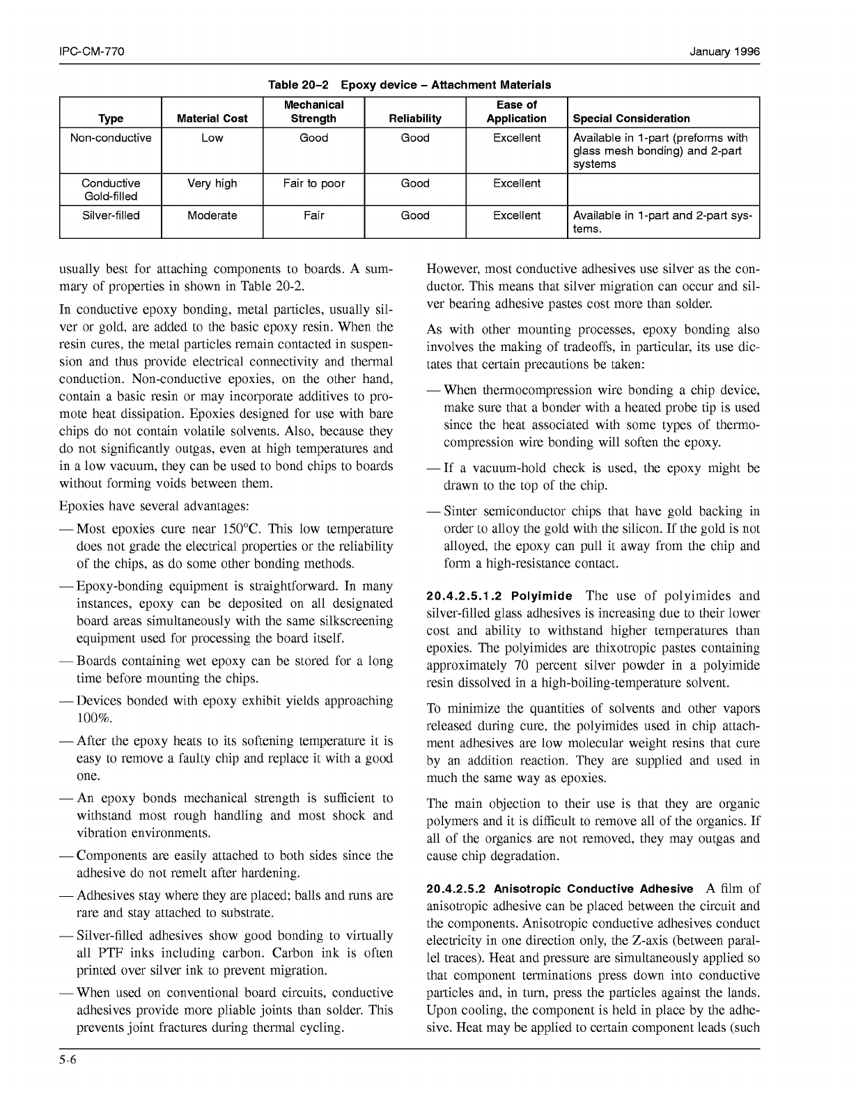
Table 20-2 Epoxy device
-
Attachment Materials
Mechanical Ease
of
Type
Special Consideration
Application Reliability Strength
Material Cost
Non-conductive Available in 1-part (preforms with Excellent Good Good Low
glass mesh bonding) and 2-part
systems
Conductive
Available in 1-part and 2-part sys- Excellent Good Fa¡ r Moderate Silver-filled
Gold-filled
Excellent Good
Fair to poor
Very high
tems.
usually best for attaching components to boards. A sum-
mary of properties in shown in Table
20-2.
In conductive epoxy bonding, metal particles, usually sil-
ver or gold, are added to the basic epoxy resin. When the
resin cures, the metal particles remain contacted in suspen-
sion and thus provide electrical connectivity and thermal
conduction. Non-conductive epoxies, on the other hand,
contain a basic resin or may incorporate additives to pro-
mote heat dissipation. Epoxies designed for use with bare
chips do not contain volatile solvents. Also, because they
do not significantly outgas, even at high temperatures and
in a low vacuum, they can be used to bond chips to boards
without forming voids between them.
Epoxies have several advantages:
-Most epoxies cure near 150°C. This low temperature
does not grade the electrical properties or the reliability
of the chips, as do some other bonding methods.
-
Epoxy-bonding equipment is straightforward. In many
instances, epoxy can be deposited on all designated
board areas simultaneously with the same silkscreening
equipment used for processing the board itself.
-Boards containing wet epoxy can be stored for a long
time before mounting the chips.
-Devices bonded with epoxy exhibit yields approaching
100%.
-After the epoxy heats to its softening temperature it is
easy to remove a faulty chip and replace it with a good
one.
-An epoxy bonds mechanical strength is sufficient to
withstand most rough handling and most shock and
vibration environments.
-Components are easily attached to both sides since the
adhesive do not remelt after hardening.
-
Adhesives stay where they are placed; balls and runs are
rare and stay attached to substrate.
-
Silver-filled adhesives show good bonding to virtually
all PTF inks including carbon. Carbon ink is often
printed over silver ink to prevent migration.
-When used on conventional board circuits, conductive
adhesives provide more pliable joints than solder. This
prevents joint fractures during thermal cycling.
However, most conductive adhesives use silver as the con-
ductor. This means that silver migration can occur and sil-
ver bearing adhesive pastes cost more than solder.
As with other mounting processes, epoxy bonding also
involves the making of tradeoffs, in particular, its use dic-
tates that certain precautions be taken:
-When thermocompression wire bonding a chip device,
make sure that a bonder with a heated probe tip is used
since the heat associated with some types of thermo-
compression wire bonding will soften the epoxy.
-If a vacuum-hold check is used, the epoxy might be
drawn to the top of the chip.
-Sinter semiconductor chips that have gold backing in
order to alloy the gold with the silicon. If the gold is not
alloyed, the epoxy can pull it away from the chip and
form a high-resistance contact.
20.4.2.5.1.2 Polyimide
The use of polyimides and
silver-filled glass adhesives is increasing due to their lower
cost and ability to withstand higher temperatures than
epoxies. The polyimides are thixotropic pastes containing
approximately
70
percent silver powder in a polyimide
resin dissolved in a high-boiling-temperature solvent.
To minimize the quantities of solvents and other vapors
released during cure, the polyimides used in chip attach-
ment adhesives are low molecular weight resins that cure
by an addition reaction. They are supplied and used in
much the same way as epoxies.
The main objection to their use is that they are organic
polymers and it is difficult to remove all of the organics. If
all of the organics are not removed, they may outgas and
cause chip degradation.
20.4.2.5.2 Anisotropic Conductive Adhesive
A film of
anisotropic adhesive can be placed between the circuit and
the components. Anisotropic conductive adhesives conduct
electricity in one direction only, the Z-axis (between paral-
lel traces). Heat and pressure are simultaneously applied
so
that component terminations press down into conductive
particles and, in turn, press the particles against the lands.
Upon cooling, the component is held in place by the adhe-
sive. Heat may be applied to certain component leads (such
5-6
COPYRIGHT Association Connecting Electronics Industries
Licensed by Information Handling Services
COPYRIGHT Association Connecting Electronics Industries
Licensed by Information Handling Services
January
1996
IPC-CM-770
as larger gull-wing types). Conversely, the circuit may be
heated by convection or direct transfer. Liquid thermoset
adhesive materials are processed differently. The material is
coated or printed onto the circuit. The entire board can be
covered. Components are conventionally placed and heat-
ing them cures the adhesive. Electrical contact is made
between the circuit and the components. The conductive
particles in the unpopulated areas remain dispersed within
the resin
so
that it serves as an insulative coating. Caution
-
use only with manufacturer’s approved component and
land surface finishes. Other finishes may lead to reliable
connections.
21
.O
THROUGH-HOLE MOUNTING TECHNIQUES
The most significant advantage of using the through-the-
board mounting method is its compatibility with conven-
tional mass soldering techniques, such as dip and wave
soldering. In addition, replacement of flatpacks mounted in
this manner is readily accomplished by melting and remov-
ing the solder from each land individually or in multiples.
Parts and components should be mounted on the side of the
printed board opposite that which would be in contact with
the solder if the board is machine soldered. Except when
mounted in cordwood modules or on nonrepairable printed
boards, parts and components should be
so
spaced and
so
located that any part can be removed from the printed
board without removing another part.
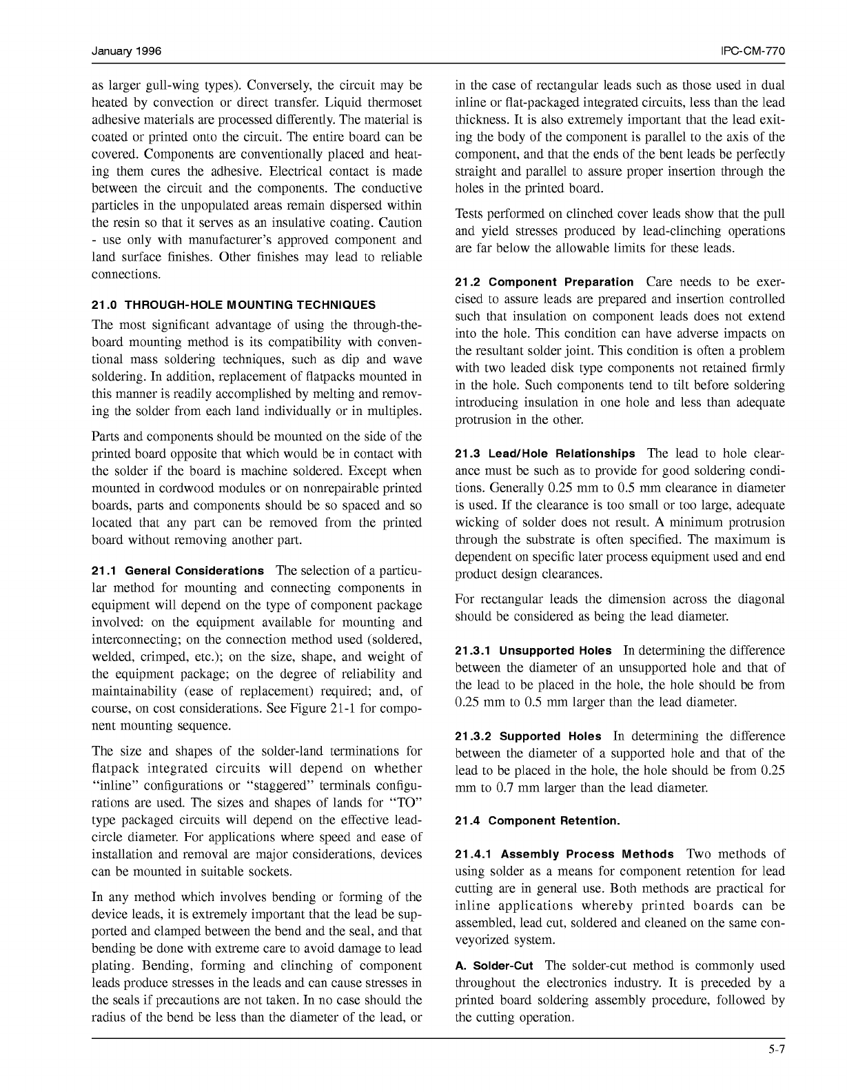
21.1 General Considerations
The selection of a particu-
lar method for mounting and connecting components in
equipment will depend on the type of component package
involved: on the equipment available for mounting and
interconnecting; on the connection method used (soldered,
welded, crimped, etc.); on the size, shape, and weight of
the equipment package; on the degree of reliability and
maintainability (ease of replacement) required; and, of
course, on cost considerations. See Figure
21-1
for compo-
nent mounting sequence.
The size and shapes of the solder-land terminations for
flatpack integrated circuits will depend on whether
“inline” configurations or “staggered” terminals configu-
rations are used. The sizes and shapes of lands for “TO”
type packaged circuits will depend on the effective lead-
circle diameter. For applications where speed and ease of
installation and removal are major considerations, devices
can be mounted in suitable sockets.
In any method which involves bending or forming of the
device leads, it is extremely important that the lead be sup-
ported and clamped between the bend and the seal, and that
bending be done with extreme care to avoid damage to lead
plating. Bending, forming and clinching of component
leads produce stresses in the leads and can cause stresses in
the seals if precautions are not taken. In no case should the
radius of the bend be less than the diameter of the lead, or
in the case of rectangular leads such as those used in dual
inline or flat-packaged integrated circuits, less than the lead
thickness. It is also extremely important that the lead exit-
ing the body of the component is parallel to the axis of the
component, and that the ends of the bent leads be perfectly
straight and parallel to assure proper insertion through the
holes in the printed board.
Tests performed on clinched cover leads show that the pull
and yield stresses produced by lead-clinching operations
are
far
below the allowable limits for these leads.
21.2 Component Preparation
Care needs to be exer-
cised to assure leads are prepared and insertion controlled
such that insulation on component leads does not extend
into the hole. This condition can have adverse impacts on
the resultant solder joint. This condition is often a problem
with two leaded disk type components not retained firmly
in the hole. Such components tend to tilt before soldering
introducing insulation in one hole and less than adequate
protrusion in the other.
21.3 LeadlHole Relationships
The lead to hole clear-
ance must be such as to provide for good soldering condi-
tions. Generally
0.25
mm to
0.5
mm clearance in diameter
is used.
If
the clearance is too small or too large, adequate
wicking of solder does not result.
A
minimum protrusion
through the substrate is often specified. The maximum is
dependent on specific later process equipment used and end
product design clearances.
For rectangular leads the dimension across the diagonal
should be considered as being the lead diameter.
21.3.1 Unsupported Holes
In determining the difference
between the diameter of an unsupported hole and that of
the lead to be placed in the hole, the hole should be from
0.25
mm to
0.5
mm larger than the lead diameter.
21.3.2 Supported Holes
In determining the difference
between the diameter of a supported hole and that of the
lead to be placed in the hole, the hole should be from
0.25
mm to
0.7
mm larger than the lead diameter.
21.4 Component Retention.
21.4.1 Assembly Process Methods
Two methods of
using solder as a means for component retention for lead
cutting are in general use. Both methods are practical for
inline applications whereby printed boards can be
assembled, lead cut, soldered and cleaned on the same con-
veyorized system.
A. Solder-Cut
The solder-cut method is commonly used
throughout the electronics industry. It is preceded by a
printed board soldering assembly procedure, followed by
the cutting operation.
5-7
COPYRIGHT Association Connecting Electronics Industries
Licensed by Information Handling Services
COPYRIGHT Association Connecting Electronics Industries
Licensed by Information Handling Services
IPC-CM-770
Januaty
1996
lncommg
receiving
I
boards
S
I
inspaclion
commnents
L
m.
Board
S
preparation
T
-
Solder
components
Misc.
componenls
-
Radial
-
-
Dips
Component
.I
l
I
I
4
I
l
I
Preclean
prebake PWB
inspection
I
l
louc,h-up
IPC-1-00384
Figure 21-1 Component Mounting Sequence
Boards may be assembled in carriers, which then move
successively over fluxer, preheaters, and soldering unit.
After soldering, boards continue to move in same carriers
to the next inline station.
B.
Solder-Cut Solder
The solder-cut solder method is
used for requirements where base metal of component
leads, exposed by lead cutting, must be solder-coated. A
second inline soldering operation is added after the inline
lead cutter. All steps, except initial carrier loading and final
unloading are automatic.
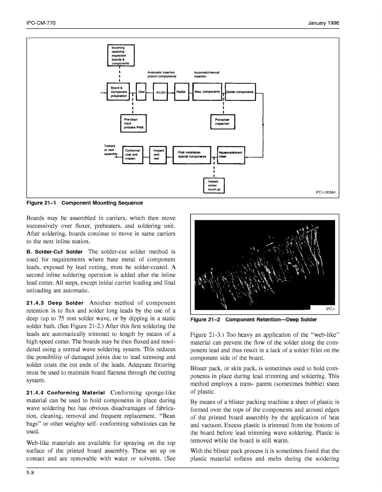
21.4.3 Deep Solder
Another method of component
retention is to flux and solder long leads by the use of a
deep (up to
75
mm solder wave, or by dipping in a static
solder bath. (See Figure
21-2.)
After this first soldering the
leads are automatically trimmed to length by means of a
high speed cutter. The boards may be then fluxed and resol-
dered using a normal wave soldering system. This reduces
the possibility of damaged joints due to lead stressing and
solder coats the cut ends of the leads. Adequate fixturing
must be used to maintain board flatness through the cutting
system.
21.4.4 Conforming Material
Conforming sponge-like
material can be used to hold components in place during
wave soldering but has obvious disadvantages of fabrica-
tion, cleaning, removal and frequent replacement. “Bean
bags” or other weighty self- conforming substitutes can be
used.
Web-like materials are available for spraying on the top
surface of the printed board assembly. These set up on
contact and are removable with water or solvents. (See
Figure 21 -2 Component Retention-Deep Solder
Figure
21-3.)
Too heavy an application of the “web-like’’
material can prevent the flow of the solder along the com-
ponent lead and thus result in a lack of a solder fillet on the
component side of the board.
Blister pack, or skin pack, is sometimes used to hold com-
ponents in place during lead trimming and soldering. This
method employs a trans- parent (sometimes bubble) sheet
of plastic.
By means of a blister packing machine a sheet of plastic is
formed over the tops of the components and around edges
of the printed board assembly by the application of heat
and vacuum. Excess plastic is trimmed from the bottom of
the board before lead trimming wave soldering. Plastic is
removed while the board is still warm.
With the blister pack process it is sometimes found that the
plastic material softens and melts during the soldering
5-8
COPYRIGHT Association Connecting Electronics Industries
Licensed by Information Handling Services
COPYRIGHT Association Connecting Electronics Industries
Licensed by Information Handling Services