IPC-CM-770D-1996.pdf - 第88页
IPC-CM-770 Januaty 1996 or circuit. Such assess is required for main- tenance and adjustment of circuitry. Use of a test point is preferable to probing the printed board, since probing a printed board can be a shock haza…
January
1996 IPC-CM-770
Current carrying capacity? (Select wire size. Table 17-1 switching circuits. In addition, because transistorized and
lists the current carrying capacity of small wires.)
integrated equipment requires relatively high currents with
Ease of handling? (Select wire size. Table 17-2 lists the
low voltages, it is essential that DC power distribution lines
breaking strength of typical small wires.)
have a low inductance and resistance with a high capaci-
tance.
17.1.4 Bus Bars
High-speed, solid-state circuits demand
distribution circuits be designed and placed with reference
area
Of
a
conductor.
to minimum noise pickup-a common source of pickup is
greater control of electrical noise. It is important that power Resistance can be reduced by increasing the cross sectional
Table 17-1 Current Carrying Capacity
of
Small Wires’
Rating for PVC
&
Similar
Low
Fusing Current Bare Wire, Rating for TFE
&
Similar High
Conductor Size AWG
Amperes
Temp Insulation. Amperes Temp. Insulation. Amperes
30
20.5 7 4 26
14.4 6 3 28
10.2 4 2
I
24
I
6
I
10
I
29.2
I
22
I
8
I
13
I
41.2
I
20
I
10
I
17
I
58.4
I
18 82.9 24 15
1.
Ratings are based on a single conductor at 30°C ambient temperature in still air. Other factors which affect the current carrying capacity of a conductor are
the length of the wire, the proximity to other wires, the cooling available, and the thickness of the insulation. Because of these variables, the data in this table
should be considered as an approximation only.
Table 17-2 Breaking Strength
of
Small Wires
Conductor Size
1.
Calculated in accordance with ASTM B-25, using an Ultimate Tensile
Strength value of 42,000 psi for annealed copper.
To obtain minimum, effective inductance, conductors must
be placed close together. In this manner, the magnetic
fields around each conductor, when
180
out of phase would
tend to cancel and reduce a possible source of noise.
Twisted pairs of wire have been used to achieve this effect-
however a twisted pair of wires has more inductance than
a laminated bus bar.
Since each flat conductor in a laminated bus bar can be
surrounded with ground shields to further reduce stray
electrical fields, the laminated bus is even more desirable
for power distribution. Moreover, the laminated bus bar
design permits maximum allowable distributed capacitance
between adjacent conductors, thereby reducing and sup-
pressing undesirable voltages, pulses, and noise.
The laminated bus bar is essentially a composite of flat
conductors isolated from each other with a dielectric mate-
rial and laminated into a rigid multiconductor unit. Due to
its physical structure, the laminated bus maintains very
definite electrical characteristics. When used as an integral
part of an electronic system it is a very stable circuit ele-
ment.
The number of conductors or levels, types and number of
terminals, size and finish of the conductor and the dielec-
tric strength required, depends upon the application.
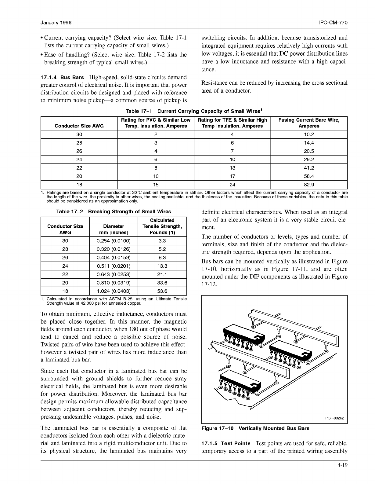
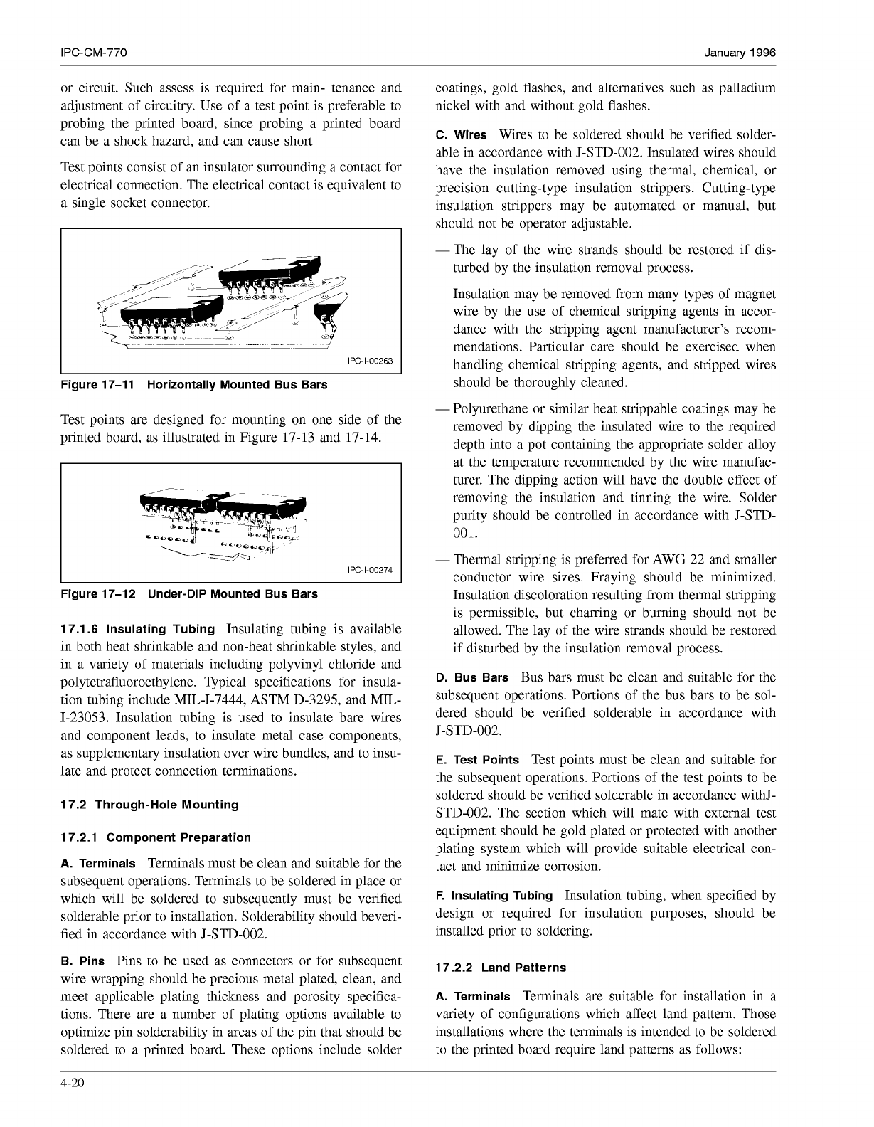
Bus bars can be mounted vertically as illustrated in Figure
17-10, horizontally as in Figure 17-11, and are often
mounted under the DIP components as illustrated in Figure
17-12.
I
IPC-1-00262
Figure 17-10 Vertically Mounted Bus Bars
17.1.5 Test Points
Test points are used for safe, reliable,
temporary access to a part of the printed wiring assembly
4-19
COPYRIGHT Association Connecting Electronics Industries
Licensed by Information Handling Services
COPYRIGHT Association Connecting Electronics Industries
Licensed by Information Handling Services
IPC-CM-770
Januaty
1996
or circuit. Such assess is required for main- tenance and
adjustment of circuitry. Use of a test point is preferable to
probing the printed board, since probing a printed board
can be a shock hazard, and can cause short
Test points consist of an insulator surrounding a contact for
electrical connection. The electrical contact is equivalent to
a single socket connector.
I
IPC-1-00263
I
Figure 17-11 Horizontally Mounted Bus Bars
Test points are designed for mounting on one side of the
printed board, as illustrated in Figure 17-13 and 17-14.
IPC-1-00274
Figure 17-12 Under-DIP Mounted Bus Bars
17.1.6 Insulating Tubing
Insulating tubing is available
in both heat shrinkable and non-heat shrinkable styles, and
in a variety of materials including polyvinyl chloride and
polytetrafluoroethylene.
Typical specifications for insula-
tion tubing include MIL-1-7444, ASTM D-3295, and MIL-
1-23053. Insulation tubing is used to insulate bare wires
and component leads, to insulate metal case components,
as supplementary insulation over wire bundles, and to insu-
late and protect connection terminations.
17.2 Through-Hole Mounting
17.2.1 Component Preparation
A.
Terminals
Terminals must be clean and suitable for the
subsequent operations. Terminals to be soldered in place or
which will be soldered to subsequently must be verified
solderable prior to installation. Solderability should beveri-
fied in accordance with J-STD-002.
B. Pins
Pins to be used as connectors or for subsequent
wire wrapping should be precious metal plated, clean, and
meet applicable plating thickness and porosity specifica-
tions. There are a number of plating options available to
optimize pin solderability in areas of the pin that should be
soldered to a printed board. These options include solder
coatings, gold flashes, and alternatives such as palladium
nickel with and without gold flashes.
C. Wires
Wires to be soldered should be verified solder-
able in accordance with J-STD-002. Insulated wires should
have the insulation removed using thermal, chemical, or
precision cutting-type insulation strippers. Cutting-type
insulation strippers may be automated or manual, but
should not be operator adjustable.
-The lay of the wire strands should be restored if dis-
turbed by the insulation removal process.
-
Insulation may be removed from many types of magnet
wire by the use of chemical stripping agents in accor-
dance with the stripping agent manufacturer's recom-
mendations. Particular care should be exercised when
handling chemical stripping agents, and stripped wires
should be thoroughly cleaned.
-
Polyurethane or similar heat strippable coatings may be
removed by dipping the insulated wire to the required
depth into a pot containing the appropriate solder alloy
at the temperature recommended by the wire manufac-
turer. The dipping action will have the double effect of
removing the insulation and tinning the wire. Solder
purity should be controlled in accordance with J-STD-
001.
-
Thermal stripping is preferred for AWG 22 and smaller
conductor wire sizes. Fraying should be minimized.
Insulation discoloration resulting from thermal stripping
is permissible, but charring or burning should not be
allowed. The lay of the wire strands should be restored
if disturbed by the insulation removal process.
D. Bus Bars
Bus bars must be clean and suitable for the
subsequent operations. Portions of the bus bars to be sol-
dered should be verified solderable in accordance with
J-STD-002.
E.
Test Points
Test points must be clean and suitable for
the subsequent operations. Portions of the test points to be
soldered should be verified solderable in accordance withJ-
STD-002. The section which will mate with external test
equipment should be gold plated or protected with another
plating system which will provide suitable electrical con-
tact and minimize corrosion.
F. Insulating Tubing
Insulation tubing, when specified by
design or required for insulation purposes, should be
installed prior to soldering.
17.2.2 Land Patterns
A.
Terminals
Terminals are suitable for installation in a
variety of configurations which affect land pattern. Those
installations where the terminals is intended to be soldered
to the printed board require land patterns as follows:
4-20
COPYRIGHT Association Connecting Electronics Industries
Licensed by Information Handling Services
COPYRIGHT Association Connecting Electronics Industries
Licensed by Information Handling Services
January
1996
IPC-CM-770
Hardware Mount
Solder Mount
IPC-1-00265
Figure 17-13 One-terminal Printed Board Test Point
IPC-1-00266
Figure 17-1
4
Two-terminal Printed Board Test Point
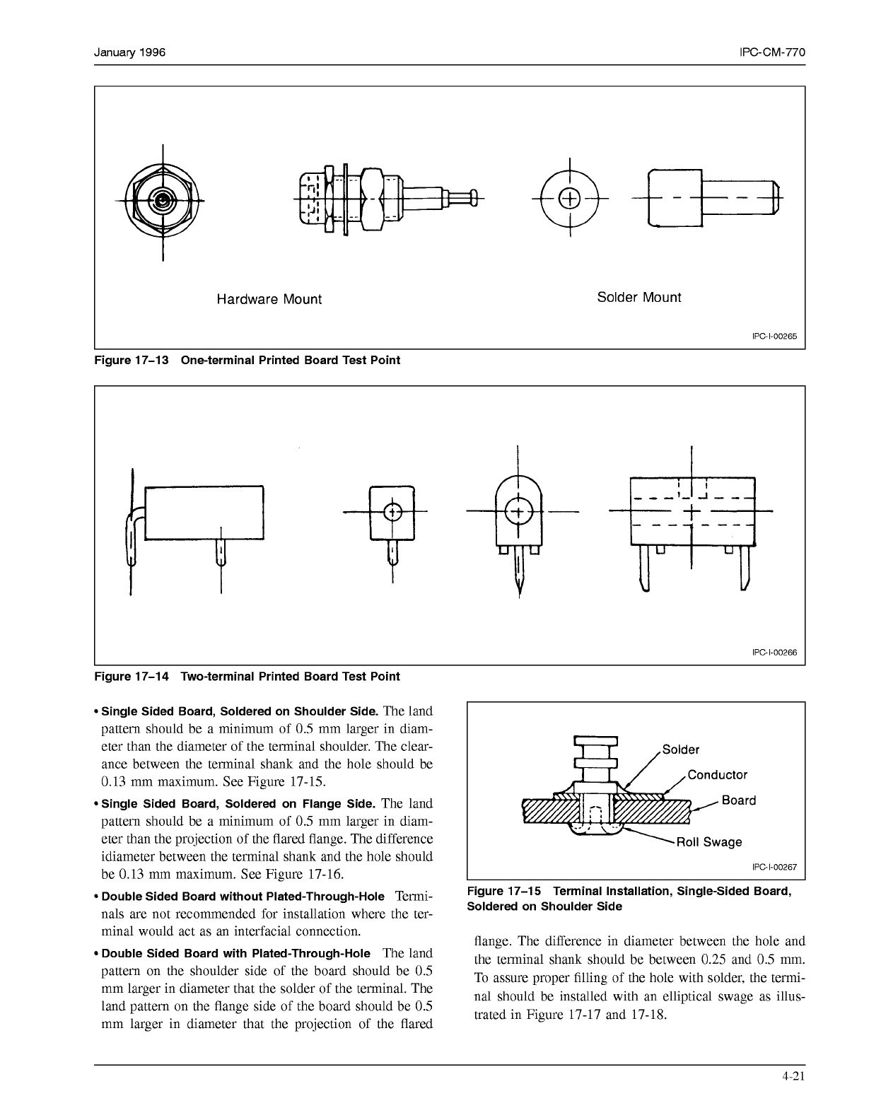
Single Sided Board, Soldered on Shoulder Side.
The land
pattern should be a minimum of
0.5
mm larger in diam-
eter than the diameter of the terminal shoulder. The clear-
ance between the terminal shank and the hole should be
0.13
mm maximum. See Figure
17-15.
Single Sided Board, Soldered on Flange Side.
The land
pattern should be a minimum of
0.5
mm larger in diam-
eter than the projection of the flared flange. The difference
idiameter between the terminal shank and the hole should
be
0.13
mm maximum. See Figure
17-16.
Double Sided Board without Plated-Through-Hole
Termi-
nals are not recommended for installation where the ter-
minal would act as an interfacial connection.
Double Sided Board with Plated-Through-Hole
The land
pattern on the shoulder side of the board should be
0.5
mm larger in diameter that the solder of the terminal. The
land pattern on the flange side of the board should be
0.5
mm larger in diameter that the projection of the flared
I
IPC-1-00267
Figure 17-15 Terminal Installation, Single-Sided Board,
Soldered on Shoulder Side
flange. The difference in diameter between the hole and
the terminal shank should be between
0.25
and
0.5
mm.
To assure proper filling of the hole with solder, the termi-
nal should be installed with an elliptical swage as illus-
trated in Figure
17-17
and
17-18.
4-21
COPYRIGHT Association Connecting Electronics Industries
Licensed by Information Handling Services
COPYRIGHT Association Connecting Electronics Industries
Licensed by Information Handling Services