IPC-CM-770D-1996.pdf - 第123页
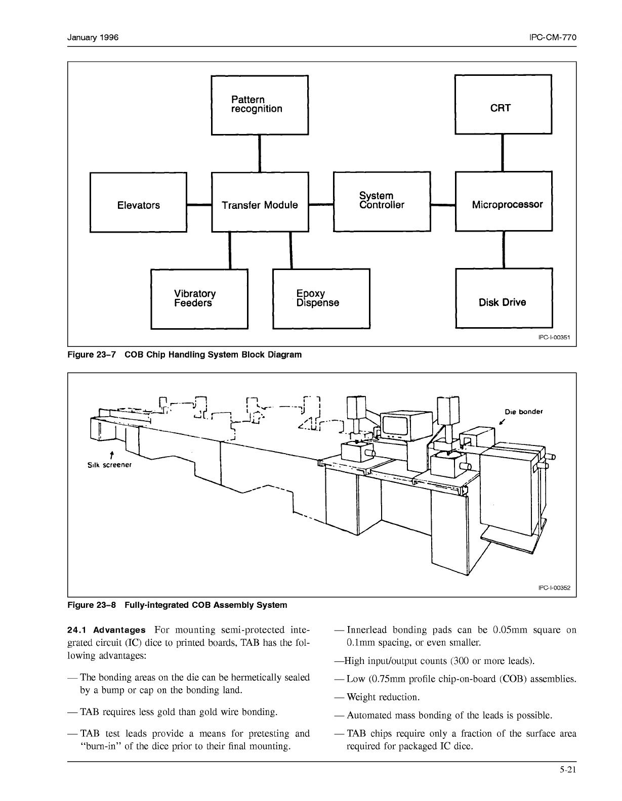
Januaw 1996 IPC-CM-770 Pattern recognition CRT System Elevators Microprocessor - Controller - Transfer Module - 1 rt)f:%y I 1 Epoxy Dispense 1 I Disk Drive 1 IPC-1-00351 Figure 23-7 COB Chip Handling System Block Diagram…
IPC-CM-770
Januaty
1996
Figure 23-4 Mechanics
of
Ultrasonic Wire Bonding
IPC-1-00339
L
Figure 23-5 Thermosonic Wedge Wire Bonding
Such a system would operate in the following manner.
First, bare boards loaded in 50-unit magazines are pre-
sented to the input feed magazine of the silkscreener,
where adhesive is deposited. Then the boards with adhesive
are automatically transferred to the pick-and-place
machine, where the chips are placed on the board over the
adhesive. The populated boards are then put back in the
magazine for further processing.
The magazines are removed from the output of the chip
attachment unit manually and put into an oven to cure the
adhesive. The boards, after curing in the magazines, are put
into the wirelead bonder's magazine feed. The chips are
then bonded to the boards and automatically put back into
I
IPC-I-
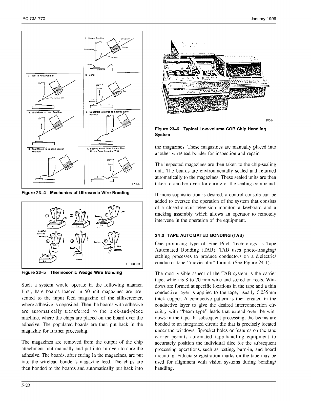
Figure 23-6 Typical Low-volume COB Chip Handling
System
the magazines. These magazines are manually placed into
another wire/lead bonder for inspection and repair.
The inspected magazines are then taken to the chip-sealing
unit. The boards are environmentally sealed and returned
automatically to the magazines. These sealed units are then
taken to another oven for curing of the sealing compound.
If
more sophistication is desired, a control console can be
added to oversee the operation of the system that consists
of a closed-circuit television monitor, a keyboard and a
tracking assembly which allows an operator to remotely
intervene in the operation of the equipment.
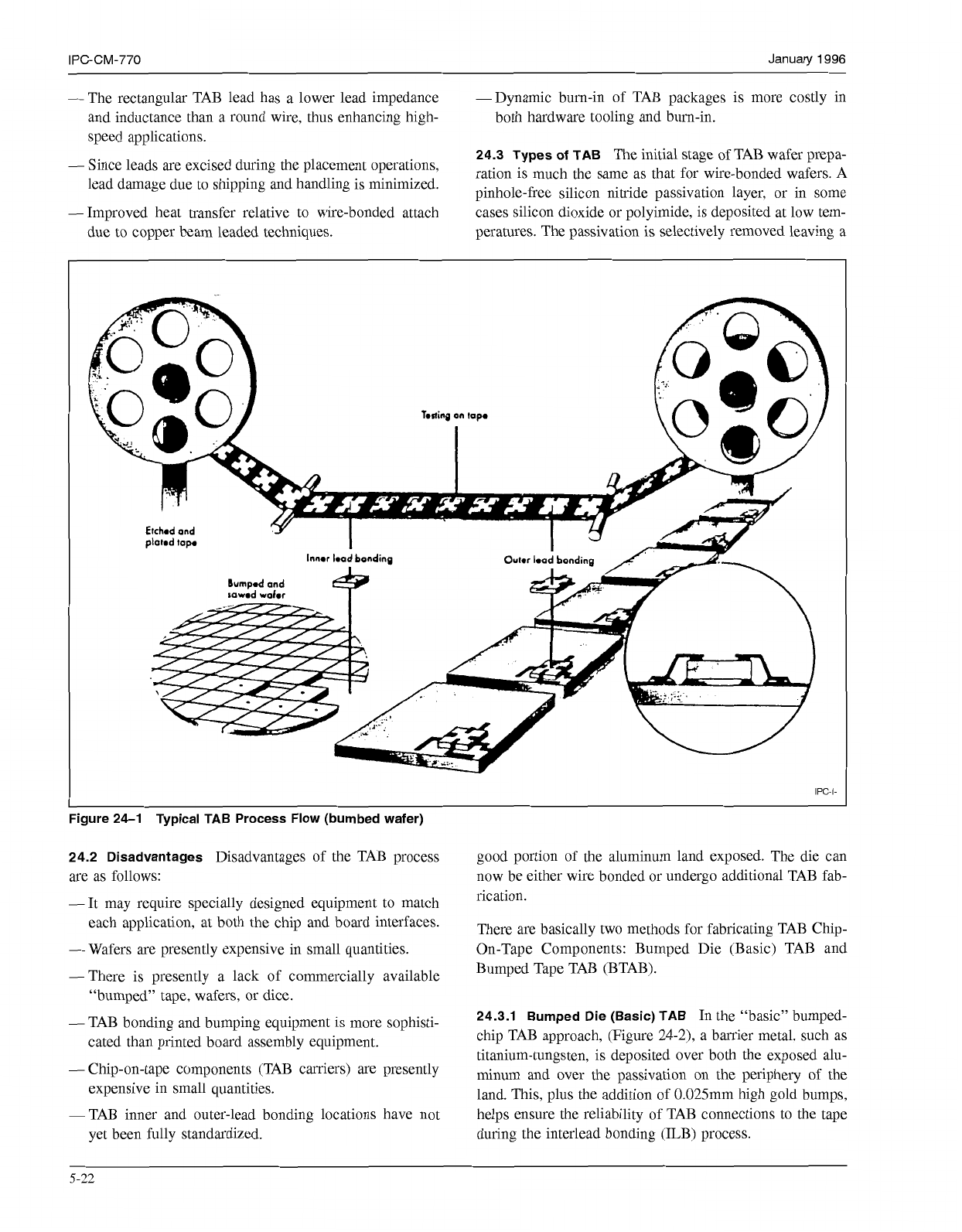
24.0 TAPE AUTOMATED BONDING (TAB)
One promising type of Fine Pitch Technology is Tape
Automated Bonding (TAB). TAB uses photo-imaging/
etching processes to produce conductors on a dielectric/
conductor tape "movie film" format. (See Figure
24-1).
The most visible aspect of the TAB system is the carrier
tape, which is
8
to
70
mm wide and stored on reels. Win-
dows are formed at specific locations in the tape and a thin
conductive layer is applied to the tape; usually 0.035mm
thick copper. A conductive pattern is then created in the
conductive layer to give the desired interconnection cir-
cuitry with "beam type" leads that extend over the win-
dows in the tape. In subsequent processing, the beams are
bonded to an integrated circuit die that is precisely located
under the windows. Sprocket holes or features on the tape
carrier permits automated tape-handling equipment to
accurately position the individual dice for the subsequent
processing operations, such as testing, bum-in, and board
mounting. Fiducials/registration marks on the tape may be
used for alignment with vision systems during bonding/
handling.
5
-20
COPYRIGHT Association Connecting Electronics Industries
Licensed by Information Handling Services
COPYRIGHT Association Connecting Electronics Industries
Licensed by Information Handling Services
Januaw
1996
IPC-CM-770
Pattern
recognition
CRT
System
Elevators
Microprocessor
-
Controller
-
Transfer Module
-
1
rt)f:%y
I
1
Epoxy
Dispense
1
I
Disk Drive
1
IPC-1-00351
Figure 23-7 COB Chip Handling System Block Diagram
IPC-1-00352
Figure 23-8 Fully-integrated COB Assembly System
24.1 Advantages
For mounting semi-protected inte- -1nnerlead bonding pads can be 0.05mm square on
grated circuit (IC) dice to printed boards, TAB has the fol- O.lmm spacing, or even smaller.
lowing advantages:
-
The bonding areas on the die can be hermetically sealed
-
LOW (0.75mm profile chip-on-board (COB) assemblies.
-High inputloutput counts
(300
or more leads).
by a bump or cap on the bonding land.
-Weight reduction.
-
TAB requires less gold than gold wire bonding.
-
Automated mass bonding of the leads is possible.
-TAB test leads provide a means for pretesting and -TAB chips require only a fraction of the surface area
“bum-in” of the dice prior to their final mounting. required for packaged IC dice.
5-21
COPYRIGHT Association Connecting Electronics Industries
Licensed by Information Handling Services
COPYRIGHT Association Connecting Electronics Industries
Licensed by Information Handling Services
IPC-CM-770
Januaty
1996
-
The rectangular TAB lead has a lower lead impedance -Dynamic bum-in of TAB packages is more costly in
and inductance than a round wire, thus enhancing high- both hardware tooling and bum-in.
speed applications.
-
Since leads are excised during the placement operations,
ration
is
much
the
Same
as
that
for
wire-bonded
wders.
A
24.3 Types of TAB
The initial stage of TAB wafer prepa-
pinhole-free silicon nitride passivation layer, or in some
-
Improved heat transfer relative to wire-bonded attach cases silicon dioxide or polyimide, is deposited at low tem-
lead damage due to shipping and handling is minimized.
due to copper beam leaded techniques.
peratures. The passivation is selectively removed leaving a
IPC-I-
Figure 24-1 Typical TAB Process Flow (bumbed wafer)
24.2 Disadvantages
Disadvantages of the TAB process
are as follows:
-It may require specially designed equipment to match
each application, at both the chip and board interfaces.
-Wafers are presently expensive in small quantities.
-There is presently a lack of commercially available
“bumped” tape, wafers, or dice.
-
TAB bonding and bumping equipment is more sophisti-
cated than printed board assembly equipment.
-
Chip-on-tape components (TAB carriers) are presently
expensive in small quantities.
-TAB inner and outer-lead bonding locations have not
yet been fully standardized.
good portion of the aluminum land exposed. The die can
now be either wire bonded or undergo additional TAB fab-
rication.
There are basically two methods for fabricating TAB Chip-
On-Tape Components: Bumped Die (Basic) TAB and
Bumped Tape TAB (BTAB).
24.3.1 Bumped Die (Basic) TAB
In the “basic” bumped-
chip TAB approach, (Figure
24-2),
a barrier metal, such as
titanium-tungsten, is deposited over both the exposed alu-
minum and over the passivation on the periphery of the
land. This, plus the addition of 0.025mm high gold bumps,
helps ensure the reliability of TAB connections to the tape
during the interlead bonding (ILB) process.
5
-22
COPYRIGHT Association Connecting Electronics Industries
Licensed by Information Handling Services
COPYRIGHT Association Connecting Electronics Industries
Licensed by Information Handling Services