IPC-CM-770D-1996.pdf - 第74页
IPC-CM-770 Januaty 1996 15.1 O Soldering Care must be taken so that flux or sol- der does not wick up into the contact. Some manufacturers provide anti-wicking devices to prevent flux or solder wicking. If connectors are…
January
1996
IPC-CM-770
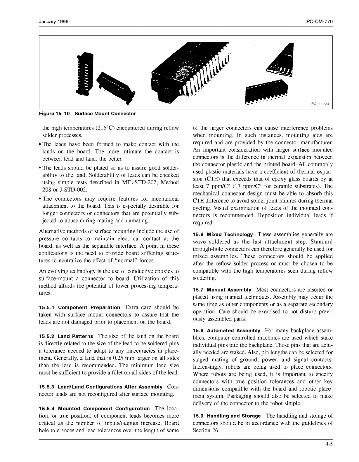
IPC-1-00234
Figure
15-1
O
Surface Mount Connector
the high temperatures (215°C) encountered during reflow
solder processes.
The leads have been formed to make contact with the
lands on the board. The more intimate the contact is
between lead and land, the better.
The leads should be plated
so
as to assure good solder-
ability to the land. Solderability of leads can be checked
using simple tests described in MIL-STD-202, Method
208 or J-STD-002.
The connectors may require features for mechanical
attachment to the board. This is especially desirable for
longer connectors or connectors that are potentially sub-
jected to abuse during mating and unmating.
Alternative methods of surface mounting include the use of
pressure contacts to maintain electrical contact at the
board, as well as the separable interface. A point in these
applications is the need to provide board stiffening struc-
tures to neutralize the effect of "normal" forces.
An evolving technology is the use of conductive epoxies to
surface-mount a connector to board. Utilization of this
method affords the potential of lower processing tempera-
tures.
15.5.1
Component Preparation
Extra care should be
taken with surface mount connectors to assure that the
leads are not damaged prior to placement on the board.
15.5.2
Land Patterns
The size of the land on the board
is directly related to the size of the lead to be soldered plus
a tolerance needed to adapt to any inaccuracies in place-
ment. Generally, a land that is 0.25 mm larger on all sides
than the lead is recommended. The minimum land size
must be sufficient to provide a fillet on all sides of the lead.
15.5.3 LeadlLand Configurations After Assembly
Con-
nector leads are not reconfigured after surface mounting.
15.5.4
Mounted Component Configuration
The loca-
tion, or true position, of component leads becomes more
critical as the number of inputs/outputs increase. Board
hole tolerances and lead tolerances over the length of some
of the larger connectors can cause interference problems
when mounting. In such instances, mounting aids are
required and are provided by the connector manufacturer.
An important consideration with larger surface mounted
connectors is the difference in thermal expansion between
the connector plastic and the printed board. All commonly
used plastic materials have a coefficient of thermal expan-
sion (CTE) that exceeds that of epoxy glass boards by at
least
7
ppm/C"
(17
ppm/C" for ceramic substrates). The
mechanical connector design must be able to absorb this
CTE difference to avoid solder joint failures during thermal
cycling. Visual examination of leads of the mounted con-
nectors is recommended. Reposition individual leads if
required.
15.6 Mixed Technology
These assemblies generally are
wave soldered as the last attachment step. Standard
through-hole connectors can therefore generally be used for
mixed assemblies. These connectors should be applied
after the reflow solder process or must be chosen to be
compatible with the high temperatures seen during reflow
soldering.
15.7
Manual Assembly
Most connectors are inserted or
placed using manual techniques. Assembly may occur the
same time as other components or as a separate secondary
operation. Care should be exercised to not disturb previ-
ously assembled parts.
15.8 Automated Assembly
For many backplane assem-
blies, computer controlled machines are used which stake
individual pins into the backplane. Those pins that are actu-
ally needed are staked. Also, pin lengths can be selected for
staged mating of ground, power, and signal contacts.
Increasingly, robots are being used to place connectors.
Where robots are being used, it is important to specify
connectors with true position tolerances and other key
dimensions compatible with the board and robotic place-
ment system. Packaging should also be selected to make
delivery of the connector to the robot simple.
15.9 Handling and Storage
The handling and storage of
connectors should be in accordance with the guidelines of
Section 26.
4-5
COPYRIGHT Association Connecting Electronics Industries
Licensed by Information Handling Services
COPYRIGHT Association Connecting Electronics Industries
Licensed by Information Handling Services
IPC-CM-770
Januaty
1996
15.1
O
Soldering
Care must be taken
so
that flux or sol-
der does not wick up into the contact. Some manufacturers
provide anti-wicking devices to prevent flux or solder
wicking.
If
connectors are not mechanically secured to the
board, suitable fixturing should be provided to prevent lift-
ing during soldering. This is especially important with
small lightweight connectors. General soldering guidelines
are discussed in Section
27.
15.1 1 Cleaning
Cleaning agents used after soldering
should not have any harmful effects upon the connector
housing material. Check with the connector manufacturer
to verify the compatibility of any cleaning agent with the
connector housing material. Any residue left on the contact
surfaces must be removed. When possible the open end of
the connector should be turned with the opening downward
so
that the cleaning agent can drain out of the connector
body to facilitate drying.
Ideally, connectors should be provided with standoffs and
should not have blind holes, to permit cleaning agent to
pass between the connector and the printed board.
15.1
2
Coating
Care must be exercised to prevent coat-
ings from getting on the contact surfaces. Wicking can
present a problem, and it may be necessary to seal around
the connector to prevent it.
cessing temperature extremes.
Two classes of sockets are available; namely, low insertion
force and zero insertion force. Low insertion force
describes disconnects where the insertionlextraction forces
associated with the normal forces and component loading
actions are present. Since the magnitude of the force is
additive and related to the number of leads per device, the
maximum size of socket is limited. In situations where high
forcelpin counts are encountered, zero insertion force con-
nectors are used. These are characterized by the presence
of a cdlever arrangement which relieves the normal force
created by the fixed spring segments of connectors.
Synonymous with this is the implication that appropriate
clearances must be provided for the camllever actuation.
The use of a socket carries the inherent cautions associated
most component namely:
Assembly reliability does not deteriorate as a result of
process incompatibility.
Contaminants are not trapped to promote the degradation
of materials in the system.
Proper selection by engineering.
Added costs.
Sockets may be classified in two categories; namely, dis-
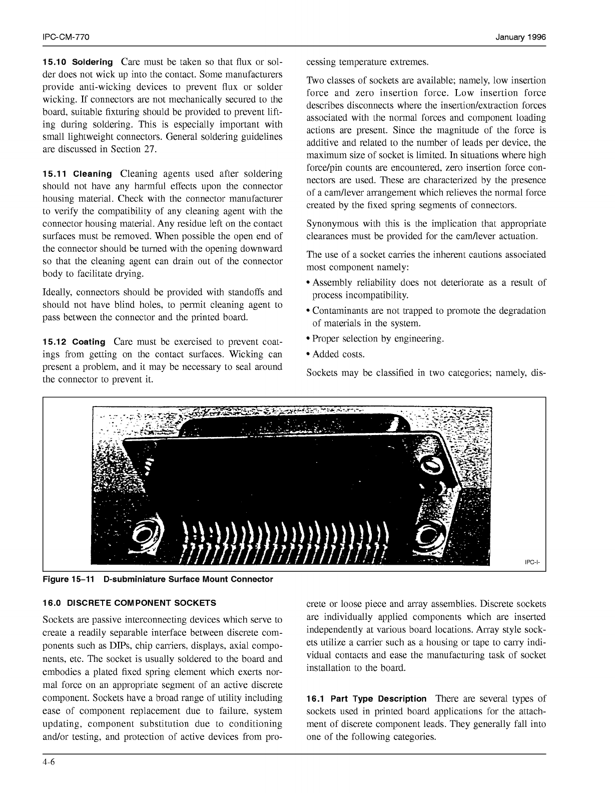
IPC-I-
L
Figure 15-11 D-subminiature Surface Mount Connector
16.0 DISCRETE COMPONENT SOCKETS
Sockets are passive interconnecting devices which serve to
create a readily separable interface between discrete com-
ponents such as DIPS, chip carriers, displays, axial compo-
nents, etc. The socket is usually soldered to the board and
embodies a plated fixed spring element which exerts nor-
mal force on an appropriate segment of an active discrete
component. Sockets have a broad range of utility including
ease of component replacement due to failure, system
updating, component substitution due to conditioning
andor testing, and protection of active devices from pro-
Crete or loose piece and array assemblies. Discrete sockets
are individually applied components which are inserted
independently at various board locations. Array style sock-
ets utilize a carrier such as a housing or tape to carry indi-
vidual contacts and ease the manufacturing task of socket
installation to the board.
16.1 Part Type Description
There are several types of
sockets used in printed board applications for the attach-
ment of discrete component leads. They generally fall into
one of the following categories.
4-6
COPYRIGHT Association Connecting Electronics Industries
Licensed by Information Handling Services
COPYRIGHT Association Connecting Electronics Industries
Licensed by Information Handling Services
January
1996
IPC-CM-770
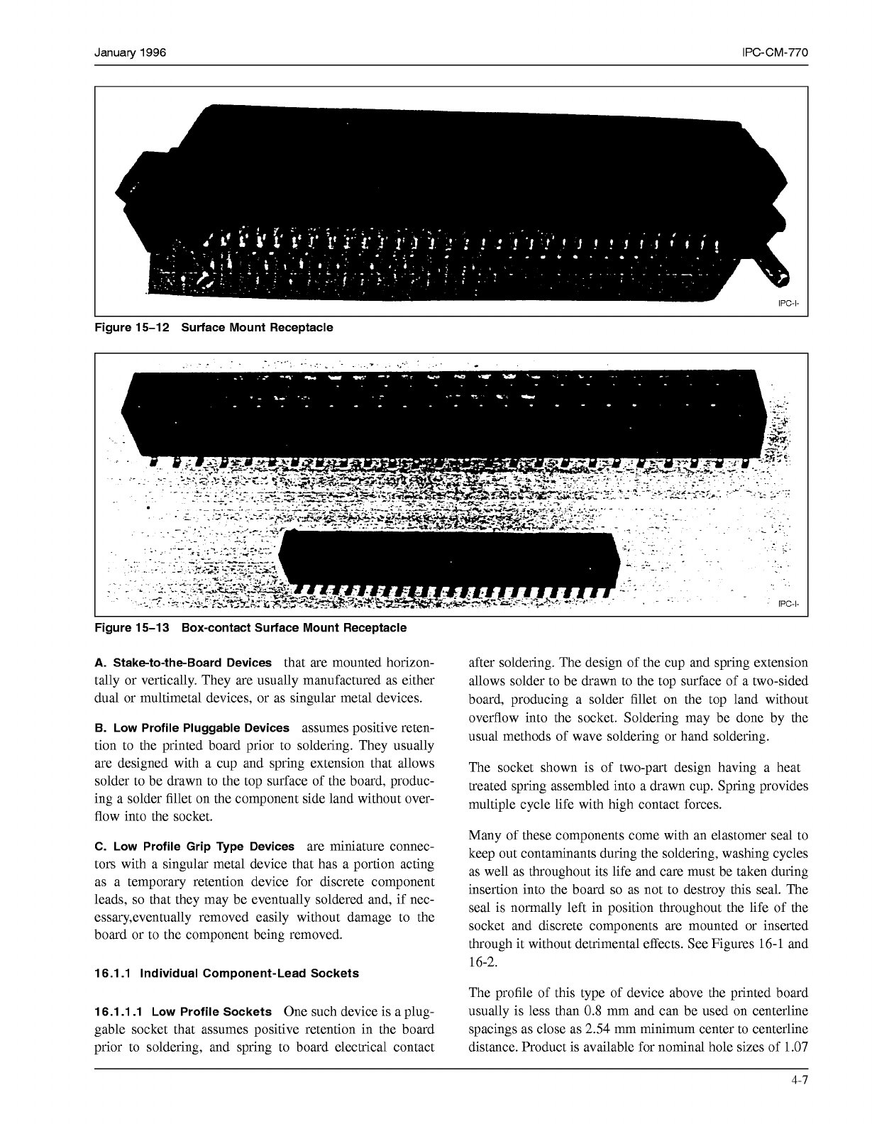
Figure 15-1
2
Surface Mount Receptacle
Figure 15-1
3
Box-contact Surface Mount Receptacle
A.
Stake-to-the-Board Devices
that are mounted horizon-
tally or vertically. They are usually manufactured as either
dual or multimetal devices, or as singular metal devices.
B. Low Profile Pluggable Devices
assumes positive reten-
tion to the printed board prior to soldering. They usually
are designed with a cup and spring extension that allows
solder to be drawn to the top surface of the board, produc-
ing a solder fillet on the component side land without over-
flow into the socket.
C. Low Profile Grip Type Devices
are miniature connec-
tors with a singular metal device that has a portion acting
as a temporary retention device for discrete component
leads,
so
that they may be eventually soldered and, if nec-
essary,eventually removed easily without damage to the
board or to the component being removed.
16.1.1 Individual Component-Lead Sockets
16.1.1.1 Low Profile Sockets
One such device is a plug-
gable socket that assumes positive retention in the board
prior to soldering, and spring to board electrical contact
after soldering. The design of the cup and spring extension
allows solder to be drawn to the top surface of a two-sided
board, producing a solder fillet on the top land without
overflow into the socket. Soldering may be done by the
usual methods of wave soldering or hand soldering.
The socket shown is of two-part design having a heat
treated spring assembled into a drawn cup. Spring provides
multiple cycle life with high contact forces.
Many of these components come with an elastomer seal to
keep out contaminants during the soldering, washing cycles
as well as throughout its life and care must be taken during
insertion into the board
so
as not to destroy this seal. The
seal is normally left in position throughout the life of the
socket and discrete components are mounted or inserted
through it without detrimental effects. See Figures 16-1 and
16-2.
The profile of this type of device above the printed board
usually is less than
0.8
mm and can be used on centerline
spacings as close as 2.54 mm minimum center to centerline
distance. Product is available for nominal hole sizes of
1.07
4-1
COPYRIGHT Association Connecting Electronics Industries
Licensed by Information Handling Services
COPYRIGHT Association Connecting Electronics Industries
Licensed by Information Handling Services