IPC-CM-770D-1996.pdf - 第32页
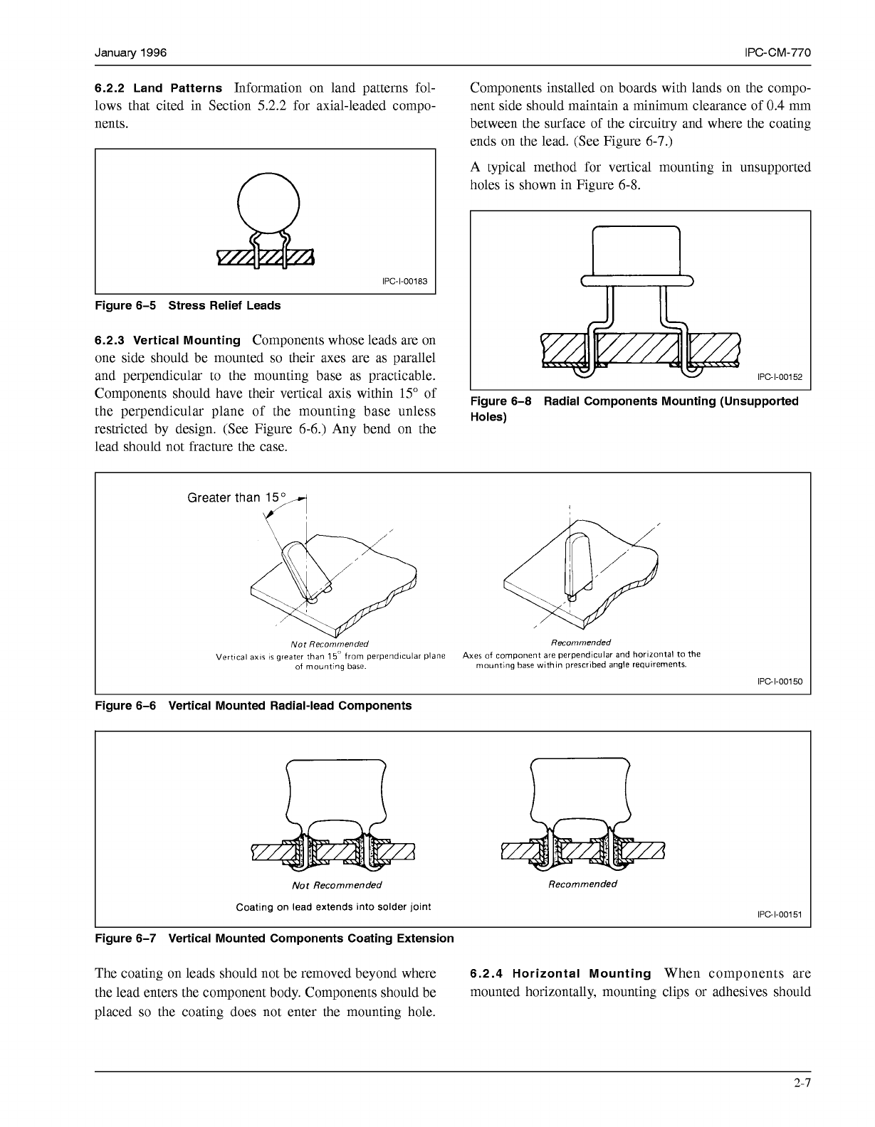
IPC-CM-770 Januaty 1996 be used. A typical method of mounting a component of this type is shown in Figure 6-9. I I 'C- I -00185 Figure 6-9 Horizontal Mounting of Radial Leaded Component 6.2.5 Metal Power Packages Me…
January
1996
IPC-CM-770
6.2.2 Land Patterns
Information on land patterns fol-
lows that cited in Section
5.2.2
for axial-leaded compo-
nents.
IPC-1-00183
I
Figure 6-5 Stress Relief Leads
6.2.3 Vertical Mounting
Components whose leads are on
one side should be mounted
so
their axes are as parallel
and perpendicular to the mounting base as practicable.
Components should have their vertical axis within
15"
of
the perpendicular plane of the mounting base unless
restricted by design. (See Figure
6-6.)
Any bend on the
lead should not fracture the case.
Components installed on boards with lands on the compo-
nent side should maintain a minimum clearance of
0.4
mm
between the surface of the circuitry and where the coating
ends on the lead. (See Figure
6-7.)
A typical method for vertical mounting in unsupported
holes is shown in Figure
6-8.
IPC-1-00152
Figure 6-8 Radial Components Mounting (Unsupported
Holes)
Greater than
15
Not
Recommended
Recornmended
Vertical
axis
is
greater than
15''
from perpendlcular plane Axes
of
component are perpendicular and
horizontal
to the
of
mountlng base. mounting base wlthln prescrlbed angle requirements.
IPC-1-00150
Figure 6-6 Vertical Mounted Radial-lead Components
Not
Recommended
Coating on lead extends into solder joint
Recommended
IPC-1-00151
Figure 6-7 Vertical Mounted Components Coating Extension
The coating on leads should not be removed beyond where
6.2.4 Horizontal Mounting
When components are
the lead enters the component body. Components should be mounted horizontally, mounting clips or adhesives should
placed
so
the coating does not enter the mounting hole.
2-7
COPYRIGHT Association Connecting Electronics Industries
Licensed by Information Handling Services
COPYRIGHT Association Connecting Electronics Industries
Licensed by Information Handling Services
IPC-CM-770
Januaty
1996
be used. A typical method of mounting a component of this
type is shown in Figure 6-9.
I I
'C-
I
-00185
Figure 6-9 Horizontal Mounting of Radial Leaded
Component
6.2.5 Metal Power Packages
Metal power packages
shown in Figure 6-10 should be mounted in accordance to
the following:
Lead holes may be plated through but should not be inter-
facial or interlayer if the component body is mounted in
contact with the board or circuitry thereon.
Component body should be spaced a minimum of 0.25
mm above the board surface if lead holes are interfacial
or interlayer (to permit solder flow to and onto the com-
ponent land).
Leads may be tempered or exceed 1.25 mm in diameter
provided they are not clinched against the printed board
land.
A washer should be inserted between each screw head
and the land (to preclude damage to the land).
A washer should be inserted between each screw head
and the board material (to preclude board damage).
Nut should be lock type or should be retained by locking
devices.
The heat sink or device mounting flange may be provided
with threads to match mounting screw for solder lug.
Resilient material and/or insulating material used as
required functionally or as standoffs.
Torque specification.
IPC-1-00049
I
L
Figure 6-1
O
Metal Power-package Transistor Mounted on
Resilient Standoffs
6.3 Surface Mounting
Radial-leaded components are
primarily suited for use in through-hole mounting technol-
ogy. However, when it is necessary to surface mount such
components, the guidelines of Section 22.1 should be fol-
lowed.
6.4 Mixed Technology
The assembly of surface mounted
devices in combination with radial-leaded through-hole
mounted devices requires two assembly processes if sur-
face mounted devices are positioned on the same printed
boards through which through-hole devices are placed. A
combination of reflow and wave solder assembly is
employed. See Section 25 for more information on mixed
assembly technology.
6.5 Manual Assembly
Procedures to be employed follow
practices to reduce contamination and damage to the com-
ponents. Identification marking is desirable on printed wir-
ing to assure proper placement of components during
assembly. Manual assembly practices as covered in Part
Five should be followed.
6.6 Automated Assembly
General information on auto-
mated techniques are covered in Part Five. Attention
should be given to control insertion forces on preformed
leads
so
as to not compromise clearance of components
from printed board surface to assure sufficient clearance for
cleaning after assembly.
6.7 Handling and Storage
The handling and storage of
radial-leaded components should be in accordance with the
guidelines of Section 26.
6.8 Soldering
General soldering techniques applying to
all types of components are described in Section 27.
6.9 Cleaning
General techniques for cleaning applying
to all types of components are described in Section 28.
6.1
O
Conformal Coating
General techniques for confor-
mal coating for all types of assemblies are described in
Section 29.
7.0 CHIP (TWO-TERMINAL) COMPONENTS
Almost every kind of two (and many three and four) termi-
nal device is available in chip component form. The most
common are chip resistors, chip capacitors and diodes but
linear magnetic devices (chokes and transformers), crystals
and even more complex devices are made in chip form.
7.1 Part Description
Chip component sizes range from
chip diodes on the order of 0.6 mm x 0.6 mm to large
capacitors that are over 9.0 mm x 2.5. Most other chip
components can be solder assembled to printed board
structures with assembly technologies similar to those
described for through-hole mounted components.
2-8
COPYRIGHT Association Connecting Electronics Industries
Licensed by Information Handling Services
COPYRIGHT Association Connecting Electronics Industries
Licensed by Information Handling Services
January
1996
IPC-CM-770
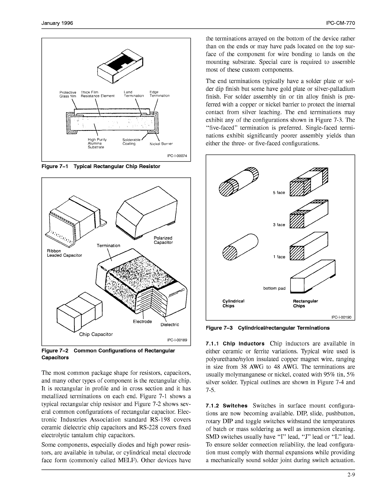
Pratectlve Thlck
Fllm
Glass
film
Reslstance Element TerminatIan Termlnatlon
Land
Edge
\
Alumna
Hlgh Purity Solderable
Substrate
Coatlng Nlckel Barrler
IPC-1-00074
Figure 7-1 Typical Rectangular Chip Resistor
Capacitor
Ribbon
Leaded Capacitor
Termination
IPC-1-00189
Figure 7-2 Common Configurations of Rectangular
Capacitors
The most common package shape for resistors, capacitors,
and many other types of component is the rectangular chip.
It is rectangular in profile and in cross section and it has
metallized terminations on each end. Figure 7-1 shows a
typical rectangular chip resistor and Figure 7-2 shows sev-
eral common configurations of rectangular capacitor. Elec-
tronic Industries Association standard RS-198 covers
ceramic dielectric chip capacitors and RS-228 covers fixed
electrolytic tantalum chip capacitors.
Some components, especially diodes and high power resis-
tors, are available in tubular, or cylindrical metal electrode
face form (commonly called MELF). Other devices have
the terminations arrayed on the bottom of the device rather
than on the ends or may have pads located on the top sur-
face of the component for wire bonding to lands on the
mounting substrate. Special care is required to assemble
most of these custom components.
The end terminations typically have a solder plate or sol-
der dip finish but some have gold plate or silver-palladium
finish. For solder assembly tin or tin alloy finish is pre-
ferred with a copper or nickel barrier to protect the internal
contact from silver leaching. The end terminations may
exhibit any of the configurations shown in Figure 7-3. The
“five-faced’’ termination is preferred. Single-faced termi-
nations exhibit significantly poorer assembly yields than
either the three- or five-faced configurations.
5
face
3 face
Cylindrical
Chips
1
face
bottom Dad
Rectangular
Chips
IPC-1-00190
Figure 7-3 Cylindricallrectangular Terminations
7.1.1 Chip Inductors
Chip inductors are available in
either ceramic or ferrite variations. Typical wire used is
polyurethanelnylon insulated copper magnet wire, ranging
in size from 38 AWG to 48 AWG. The terminations are
usually molymanganese or nickel, coated with 95% tin,
5%
silver solder. Typical outlines are shown in Figure 7-4 and
7-5.
7.1.2 Switches
Switches in surface mount configura-
tions are now becoming available. DIP, slide, pushbutton,
rotary DIP and toggle switches withstand the temperatures
of batch or mass soldering as well as immersion cleaning.
SMD switches usually have
“I”
lead,
“J”
lead or
“L”
lead.
To ensure solder connection reliability, the lead configura-
tion must comply with thermal expansions while providing
a mechanically sound solder joint during switch actuation.
2-9
COPYRIGHT Association Connecting Electronics Industries
Licensed by Information Handling Services
COPYRIGHT Association Connecting Electronics Industries
Licensed by Information Handling Services