IPC-CM-770D-1996.pdf - 第62页
IPC-CM-770 Januaty 1996 Table 13-2 BGA Solder Sphere Dimensions and Package Coplanarity All Dimensions are in mm. aaa =Coplanarity of solder spheres bbb =Coplanarity of BT substrate ccc =Coplanarity of overmolding AI = H…
January
1996
IPC-CM-770
The interconnections between the package and the sub-
strate (Printed Wiring Board structure) is typically made
with a solder pillar connecting the lands on the bottom of
the package and a set of matching lands on the substrate.
There are two common ways of forming the solder pillars.
In Ball Grid Arrays (BGA) an eutectic or near eutectic sol-
der ball is fused to the pads on the bottom of the package
during package manufacture. In assembly the solder balls
are reflow soldered to the substrate lands (with the assis-
tance of flux or solder paste). Since the solder ball is mol-
ten during assembly, the package has a tendency to self
center on the footprint producing a very robust assembly
process. The height of the solder pillar is determined by the
solder ball volume and the weight of the package. Ball
Grid Arrays are most common in plastic body packages.
In Column Grid Arrays (CGA) The solder pillars are cast
directly onto the package lands out of a high melting point
solder. They are soldered to the substrate footprint with
solder paste
so
that only the very bottom and the pillars
reflow. This provides a controlled height of the solder col-
umn (with an accompanying increase in fatigue lifetime) at
the cost of a less robust assembly procedure. CGAs are
most common in ceramic body packages.
The material in this section is specific to plastic packages
which have been registered under JEDEC. While ceramic
LGA packages are offered as custom devices by some sup-
pliers, they are not yet registered with the EIA and neither
design nor reliability information is available on them.
13.2.1 Ball Grid Arrays (BGA).
Surface Mount Plastic Ball Grid Array (PBGA or BGA)
packages are considered an alternative to finer pitch, higher
I/O packages. The packages is typically an overmolded, BT
resin glass/epoxy substrate. The BGA package distributes
the pin outs over the bottom of the package and are solder
assembled to a complimentary area array of lands on a
printed circuit board. The pin-outs are typically 30 mil
diameter solder spheres that are reflowed onto the pads of
the package. BGAs provide high I/O per unit area of pack-
age, are compatible with existing SMT assembly process,
reduce PWB and component requirements and improve
manufacturing yields. Because of these advantages over
peripheral leaded devices BGAs are receiving a lot of
attention.
Specific configuration details of Ball Grid Array packages
can differ due to package performance requirements. Over-
all, the package outline the assembly methods are common.
BGAs have been registered under the JEDEC JC-11 proce-
dures of the EIA.
13.2.1.1 Summary
of
BGA Requirement and Recom-
mendations
Solder joints shall not be touched up. Via-In-
Pad (VIP) technology shall not be used at present. PWB
footprint shall have circular lands matching each termina-
tion on the BGA package. The diameter of the PWB land
should be the same as the land on BGA.
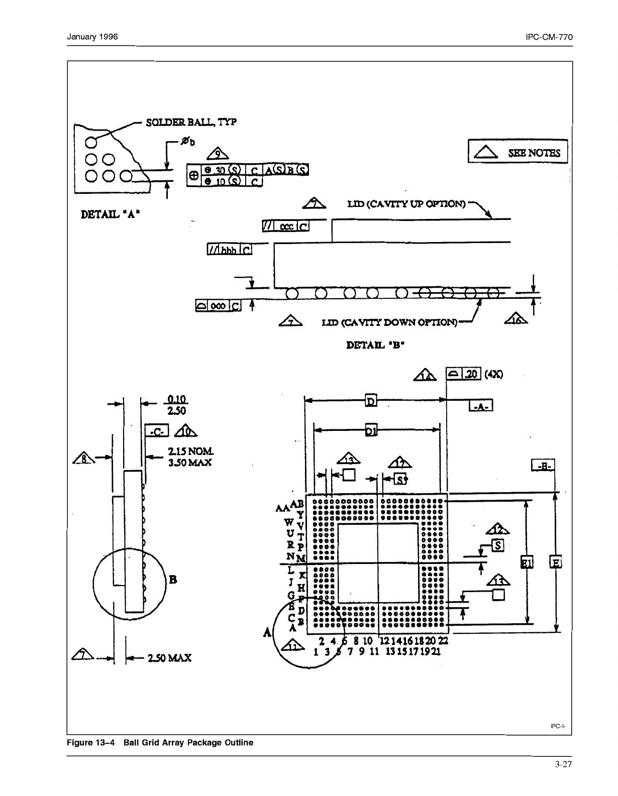
13.2.1.2 Package Drawings
Figure 13-4 contains pack-
age outline drawings for plastic BGAs taken from the
JEDEC JC-11 registration documentation. The body sizes
are “Hard Metric” and are for square bodies with sym-
metrical array. The range of package sizes, pitches and the
maximum number of I/O allowed for that pitch are con-
tained in Table 13-1.
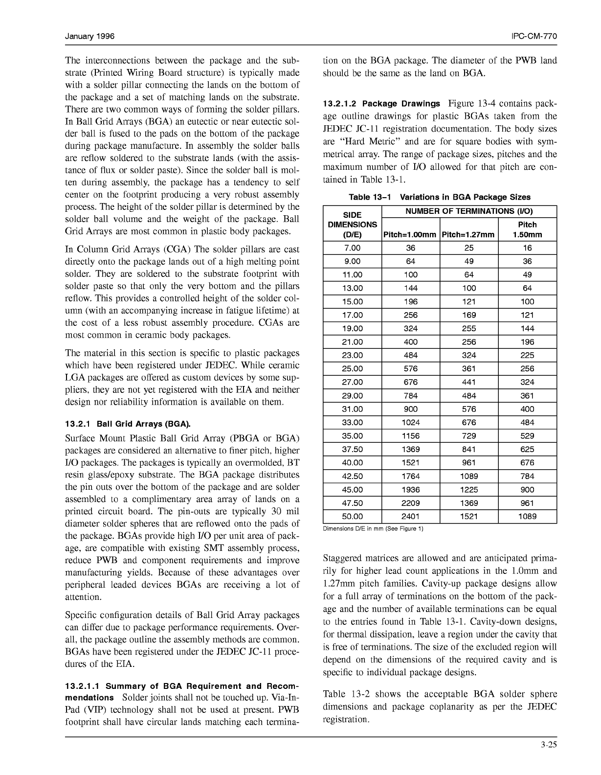
Table 13-1 Variations in BGA Package Sizes
Dimensions DIE in mm (See Figure
1)
Staggered matrices are allowed and are anticipated prima-
rily for higher lead count applications in the l.Omm and
1.27mm pitch families. Cavity-up package designs allow
for a full array of terminations on the bottom of the pack-
age and the number of available terminations can be equal
to the entries found in Table 13-1. Cavity-down designs,
for thermal dissipation, leave a region under the cavity that
is free of terminations. The size of the excluded region will
depend on the dimensions of the required cavity and is
specific to individual package designs.
Table 13-2 shows the acceptable BGA solder sphere
dimensions and package coplanarity as per the JEDEC
registration.
3-25
COPYRIGHT Association Connecting Electronics Industries
Licensed by Information Handling Services
COPYRIGHT Association Connecting Electronics Industries
Licensed by Information Handling Services
IPC-CM-770
Januaty
1996
Table 13-2 BGA Solder Sphere Dimensions and Package Coplanarity
All
Dimensions are in mm.
aaa =Coplanarity of solder spheres
bbb =Coplanarity of
BT
substrate
ccc =Coplanarity of overmolding
AI
=
Height of reflowed solder sphere on packaging
b
=
Solder sphere diameter
13.2.1.3 Assembly
BGA assembly has been proven to be consistent with the
best current practices (BCP) for surface mount (SM)
assembly. They can be assembled concurrently with periph-
eral leaded devices on a typical automated assembly line.
Paste is printed, packages are placed and then the boards
are reflowed. Reflow is typically done in an IRIConvection
oven with a nitrogen atmosphere with a profile similar to
those used for SM assembly. The assembly process of the
BGA is robust because the package tends to self center
during reflow and the molten ball can accommodate to
board or package planarity variations. Packages are avail-
able in trays or tape and reel and can be placed with stan-
dard placement machinery without special considerations.
They are currently a class
3
component and require special
handling. They must be used within 24 hours of their
removal from dry pack and must be stored in low humid-
ity once opened. The solder process is very robust for
BGAs.
Solder paste should be applied using a stencil having an
aperture of no greater than the pad diameter on all lands
with a stencil thickness no less than
6
mils. The assembly
process is relatively insensitive to solder paste thickness as
long as planarity is good enough for the solder paste to
make contact with both package and land.
Only the outer ring of solder terminations is accessible for
visual inspection. This along with measuring the collapse
of the package onto the board (approximately a 20 mil
standoff) is generally adequate for process control but does
not allow
100%
visual inspection of solder joints.
Repair can only be accomplished by total removal and
replacement of the BGA package. This can be done with
standard hot gas removal and replacement of the BGA
package. Solder joints shall NOT be touched up.
14.0 UNPACKAGED SEMICONDUCTOR COMPONENTS
There are several ways to package and assemble integrated
circuits (IC) on printed boards, see Figure 14-1.
The benefit of using Chip On Board (COB) technology all
stems from the absence of the IC package. The wire
bonded bare IC chip, COB, takes up about 114 of the area
of a Dual Inline Package (DIP) and is more space efficient
that Leadless Chip Carrier (LCC) packages. Lower profile
COB can be used in applications not possible with other
packaged chips, such as in “smart” credit cards. Trends in
low power CMOS type semi- conductor technology have
paved the way for the power limited COB technology.
14.1 Part Type Description
Semiconductor dice (chip)
types used in COB technology are comprised of back-
bonded chips and front bonded chips.
14.1.1 Back-Bonded Semiconductor Chips
Back-
bonded chips are components that install into discrete
packages. For example, in transistors the bottom of the
chip serves as the collector an metal lands serve as the base
and emitter. The chip’s collector is bonded directly to the
mounting substrate and discrete connections are made to
the base and emitter. For chip-on-board (COB) application,
chip-and-wire technology is ideally suited for use with the
back-bonded chips. The use of back-bonded chips has
advantages and disadvantages.
The advantages of using back-bonded chips are:
Availability: Most discrete IC come in chip form.
Small sizelhigh packaging densities.
Heat transfer: Intimate contact heat dissipation.
Cost: No additional processing by IC manufacturer.
The disadvantages of using back-bonded chips are:
Handling and testing is difficult due to small size.
Fragility: Susceptible to handling damage.
14.1.2 Face Bonded Semiconductor Chips
Face-
bonded chips have supplementary features that provide
access to its inputloutput lands. For COB applications,
common forms of these components include beam-tape,
TAB devices and flip chips. The use of face-bonded chips
has several advantages and disadvantages.
The advantages of using face-bonding chips are:
Mounting: Bonded circuit connections to metallization
accomplishes both mechanical mounting and electrical
3-26
COPYRIGHT Association Connecting Electronics Industries
Licensed by Information Handling Services
COPYRIGHT Association Connecting Electronics Industries
Licensed by Information Handling Services
January
1996
IPC-CM-770
O00
%
-1
DETAXL
*A8
-m
1'
4
B
A
"i
r.
1
I
r
B6
A
I
7
9
Il
131S17192l
8
10
'12141618202
00660000000
iooooreo0.o
ooomw~o+ooo
mrw~~mooo~~
oomommmommo
maommmooooo
~e~oooooooo
ooeommomaao
eo00
0.00
o000
0000
OOOC
o...
0.00
eo00
.OSO
sees
aamm
000.
m...
00eo
00.0
.amo
00.0
OO*O
oooemo
oommoeoooeo
"i
7
'Q
t
IPC-I-
Figure 13-4 Ball Grid Array Package Outline
3-27
COPYRIGHT Association Connecting Electronics Industries
Licensed by Information Handling Services
COPYRIGHT Association Connecting Electronics Industries
Licensed by Information Handling Services