IPC-CM-770D-1996.pdf - 第41页
January 1996 IPC-CM-770 method. The radial method requires a clearance around the body diameter of approximately 2.0 mm larger than the body. FRONT VIEW PLAN VIEW .O70 4 4 .O70 Spacing on two-lead side may be .100/.125&q…
IPC-CM-770
Januaty
1996
Lead bend radius requirements should also be followed
when mounting these devices.
8.2.4.3 Electrical Insulators and Thermal Conductors
When electrical insulators are also thermal conductors, the
device mounted on thermal conductors should have a maxi-
mum space of
0.05
mm between the transistor and thermal
conductor, and between the thermal conductor and the
board. However, the transistor should be in contact with the
electrical insulator/thermal conductor and the electrical
insulator/thermal conductor should be in contact with the
board at some point.
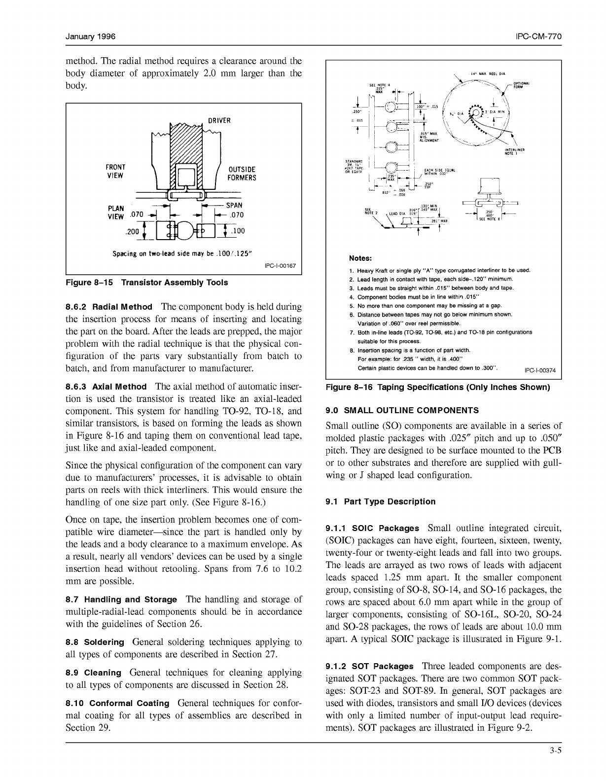
SIDE VIEW
I
END VIEW
IPC-1-00153
I
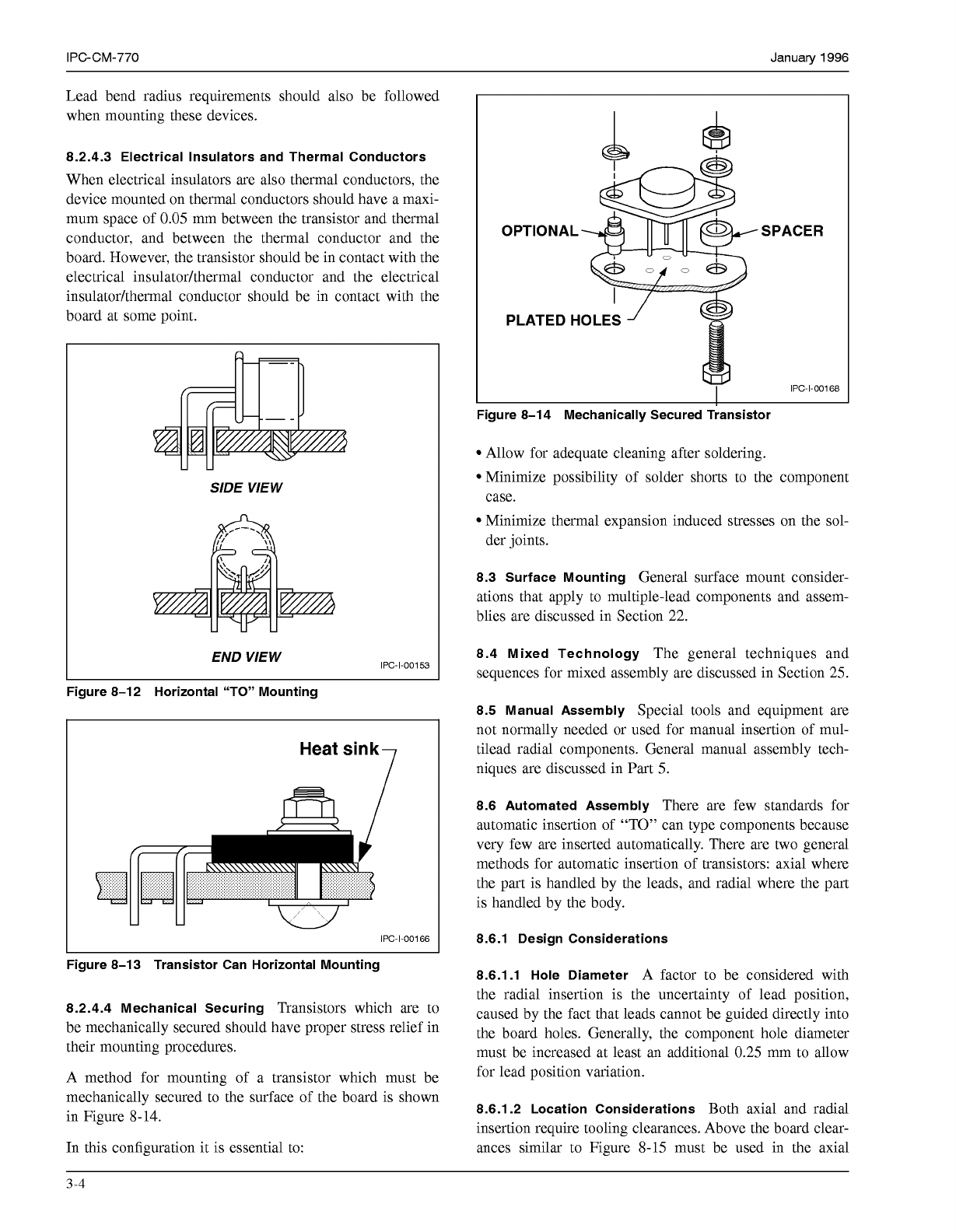
OPTIONAL SPACER
Figure 8-14 Mechanically Secured Transistor
Allow for adequate cleaning after soldering.
Minimize possibility of solder shorts to the component
case.
Minimize thermal expansion induced stresses on the sol-
der joints.
8.3 Surface Mounting
General surface mount consider-
ations that apply to multiple-lead components and assem-
blies are discussed in Section
22.
8.4 Mixed Technology
The general techniques and
sequences for mixed assembly are discussed in Section
25.
Figure 8-1 2 Horizontal “TO” Mounting
8.5 Manual Assembly
Special tools and equipment are
not normally needed or used for manual insertion of mul-
tilead radial components. General manual assembly tech-
niques are discussed in Part
5.
U U
W
IPC-1-00166
I
8.6 Automated Assembly
There are few standards for
automatic insertion of “TO” can type components because
very few are inserted automatically. There are two general
methods for automatic insertion of transistors: axial where
the part is handled by the leads, and radial where the part
is handled by the body.
8.6.1 Design Considerations
Figure 8-1 3 Transistor Can Horizontal Mounting
8.2.4.4 Mechanical Securing
Transistors which are to
be mechanically secured should have proper stress relief in
their mounting procedures.
A method for mounting of a transistor which must be
mechanically secured to the surface of the board is shown
in Figure
8-14.
In this configuration it is essential to:
8.6.1.1 Hole Diameter
A factor to be considered with
the radial insertion is the uncertainty of lead position,
caused by the fact that leads cannot be guided directly into
the board holes. Generally, the component hole diameter
must be increased at least an additional
0.25
mm to allow
for lead position variation.
8.6.1.2 Location Considerations
Both axial and radial
insertion require tooling clearances. Above the board clear-
ances similar to Figure
8-15
must be used in the axial
3-4
COPYRIGHT Association Connecting Electronics Industries
Licensed by Information Handling Services
COPYRIGHT Association Connecting Electronics Industries
Licensed by Information Handling Services
January
1996
IPC-CM-770
method. The radial method requires a clearance around the
body diameter of approximately 2.0 mm larger than the
body.
FRONT
VIEW
PLAN
VIEW
.O70
4
4
.O70
Spacing
on
two-lead
side
may
be
.100/.125"
IPC-1-00167
L
Figure 8-15 Transistor Assembly Tools
8.6.2 Radial Method
The component body is held during
the insertion process for means of inserting and locating
the part on the board. After the leads are prepped, the major
problem with the radial technique is that the physical con-
figuration of the parts vary substantially from batch to
batch, and from manufacturer to manufacturer.
8.6.3 Axial Method
The axial method of automatic inser-
tion is used the transistor is treated like an axial-leaded
component. This system for handling TO-92, TO-18, and
similar transistors, is based on forming the leads as shown
in Figure 8-16 and taping them on conventional lead tape,
just like and axial-leaded component.
Since the physical configuration of the component can vary
due to manufacturers' processes, it is advisable to obtain
parts on reels with thick interliners. This would ensure the
handling of one size part only. (See Figure 8-16.)
Once on tape, the insertion problem becomes one of com-
patible wire diameter-since the part is handled only by
the leads and a body clearance to a maximum envelope. As
a result, nearly all vendors' devices can be used by a single
insertion head without retooling. Spans from 7.6 to 10.2
mm are possible.
8.7 Handling and Storage
The handling and storage of
multiple-radial-lead components should be in accordance
with the guidelines of Section 26.
8.8 Soldering
General soldering techniques applying to
all types of components are described in Section 27.
8.9 Cleaning
General techniques for cleaning applying
to all types of components are discussed in Section 28.
8.10 Conformal Coating
General techniques for confor-
mal coating for all types of assemblies are described in
Section 29.
Notes:
1. Heavy Kraft
or
single ply
"A*
type corrugated interliner to be used.
2. Lead length in contact with tape, each side-,120" minimum.
3.
Leads must be straight within ,015" between body and tape.
4.
Component bodies
must
be in line withil .015"
5.
No
more than one component may be missing at a gap.
6.
Distance between tapes may not go below minimum shown.
Variation of
,060"
over reel permisslble.
7.
Both In-line leads (TO-92, TO-98, etc.) and TO-18 pin conflgurations
suitable for this process.
8. Insertion spacmg
IS
a function of part width.
For example: for
,235
"
width, it is
,400'
Certain plastlc devices can be handled down to
300'.
IPC-1-00374
L
Figure 8-16 Taping Specifications (Only Inches Shown)
9.0 SMALL OUTLINE COMPONENTS
Small outline
(SO)
components are available in a series of
molded plastic packages with .025" pitch and up to
.050"
pitch. They are designed to be surface mounted to the PCB
or to other substrates and therefore are supplied with gull-
wing or
J
shaped lead configuration.
9.1 Part Type Description
9.1.1 SOIC Packages
Small outline integrated circuit,
(SOIC) packages can have eight, fourteen, sixteen, twenty,
twenty-four or twenty-eight leads and fall into two groups.
The leads are arrayed as two rows of leads with adjacent
leads spaced 1.25 mm apart. It the smaller component
group, consisting of SO-8, SO-14, and SO-16 packages, the
rows are spaced about 6.0 mm apart while in the group of
larger components, consisting of S0-16L, SO-20, SO-24
and SO-28 packages, the rows of leads are about
10.0
mm
apart. A typical SOIC package is illustrated in Figure 9-1.
9.1.2 SOT Packages
Three leaded components are des-
ignated SOT packages. There are two common SOT pack-
ages: SOT-23 and SOT-89. In general, SOT packages are
used with diodes, transistors and small I/O devices (devices
with only a limited number of input-output lead require-
ments). SOT packages are illustrated in Figure 9-2.
3-5
COPYRIGHT Association Connecting Electronics Industries
Licensed by Information Handling Services
COPYRIGHT Association Connecting Electronics Industries
Licensed by Information Handling Services
IPC-CM-770
Januaty
1996
view
+
7
4
040 150
tt
4
L-
o12
SO-16
(INCHES
SHOWN)
IPC-1.00375
Figure 9-1 SO-1 6 Package Drawings Typical Dimension
9.1.3 Outlines
SO
package are included in JEDEC
95-83.
9.2 Through-Hole Mounting
so
devices are not
designed for through-hole mounting.
9.3 Surface Mounting
9.3.1 Component Preparation
SO
devices are supplied
by the manufacturers preformed for surface mounting.
Lead configurations are illustrated in Figures 9-1 and 9-2.
9.3.2 Land Patterns
Land pattern configurations for
small outline packages are provided in IPC-SM-782.
The SOT-23 package is the most common three leaded sur-
face mount device configuration. SO-89 packages are used
for high power devices where heat transfer to the support-
ing printed board is important.
With an SOT-23, the single land on one side of the pack-
age can be enlarged when reflow soldering is used,
so
that
the solder-lead surface tension is more nearly balanced.
When wave soldering is used the parts are held onto the
board with an adhesive and the surface tension balance is
not important.
9.3.3 LeadlLand Configuration After Assembly
so
devices may be mounted with or without adhesive.
If
adhe-
sive is used to secure the
SO
package to the substrate,
major considerations are:
The adhesive must not contaminate the land area.
The adhesive must be cured prior to soldering
9.3.4 Mounted Component Configurations
Applicable
guidelines are included in Section 22.
9.4 Mixed Technology
Higher count
SO
devices are nor-
mally mounted on the component side of the substrate
while the small SOT devices can be found on both sides.
Therefore, the guidelines of Section 25 are the usual
method of fabrication when the assembly uses both
SO
devices and through-the-board mounted devices.
9.5 Manual Assembly
Manual techniques for assembly
using
SO
devices are included in Section 22.
9.6 Automated Assembly
Automated techniques for
assembly using
SO
devices are included in Section 22.
9.7 Handling and Storage
The handling and storage of
small-outline components should be in accordance with the
guidelines of Section 26.
9.8 Soldering
General soldering techniques applying to
all types of components are described in Section 27.
9.9 Cleaning
General techniques for cleaning applying
to all types of components are described in Section 28.
9.1
O
Conformal Coating
General techniques for confor-
mal coating for all types of assemblies are described in
Section 29.
10.0 INLINE-LEAD COMPONENTS
10.1
Part Type Description
10.1.1 Dual-lnline Packages
The dual inline multiple-
lead component (DIP) has its lead pointing downward
ready for insertion into holes in a printed board.
The dual inline package can be inserted easily, either auto-
matically or manually. Sockets are available for mounting
and testing purposes. Automatic insertion is very feasible
using this package configuration.
A DIP is made of metal, ceramic, glass, plastic, or combi-
nations of these materials. Leads, body, and glass sealing
are designed to make this a rugged package. Lead configu-
ration (shoulder) provides a standoff feature. Leads formed
3-6
COPYRIGHT Association Connecting Electronics Industries
Licensed by Information Handling Services
COPYRIGHT Association Connecting Electronics Industries
Licensed by Information Handling Services