IPC-CM-770D-1996.pdf - 第111页
January 1996 - IPC-CM-770 Figure 21-3 Conforming Web-like Material operation and it then adheres to the components leads, making it difficult to remove. 21.4.5 Wax Stabilizing Stabilizing is a method by which long and sh…
IPC-CM-770
Januaty
1996
lncommg
receiving
I
boards
S
I
inspaclion
commnents
L
m.
Board
S
preparation
T
-
Solder
components
Misc.
componenls
-
Radial
-
-
Dips
Component
.I
l
I
I
4
I
l
I
Preclean
prebake PWB
inspection
I
l
louc,h-up
IPC-1-00384
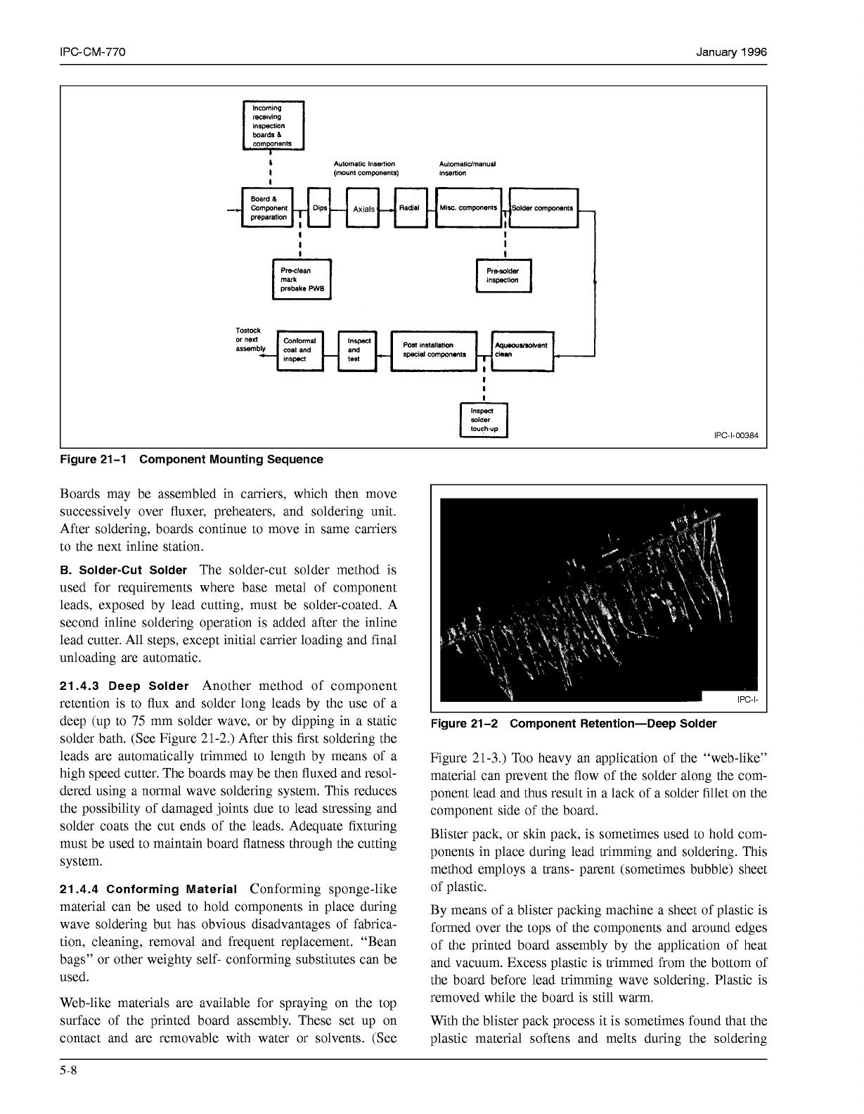
Figure 21-1 Component Mounting Sequence
Boards may be assembled in carriers, which then move
successively over fluxer, preheaters, and soldering unit.
After soldering, boards continue to move in same carriers
to the next inline station.
B.
Solder-Cut Solder
The solder-cut solder method is
used for requirements where base metal of component
leads, exposed by lead cutting, must be solder-coated. A
second inline soldering operation is added after the inline
lead cutter. All steps, except initial carrier loading and final
unloading are automatic.
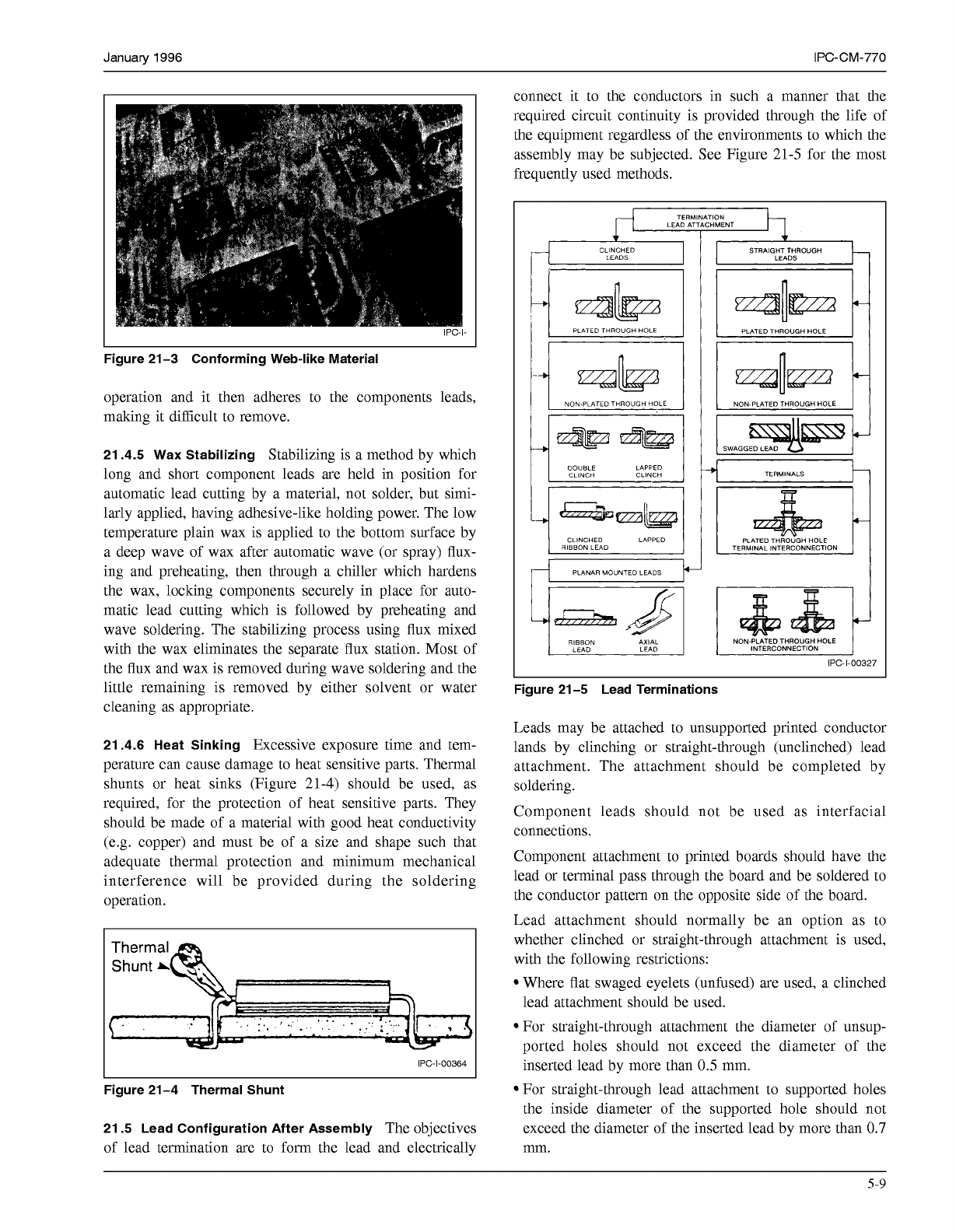
21.4.3 Deep Solder
Another method of component
retention is to flux and solder long leads by the use of a
deep (up to
75
mm solder wave, or by dipping in a static
solder bath. (See Figure
21-2.)
After this first soldering the
leads are automatically trimmed to length by means of a
high speed cutter. The boards may be then fluxed and resol-
dered using a normal wave soldering system. This reduces
the possibility of damaged joints due to lead stressing and
solder coats the cut ends of the leads. Adequate fixturing
must be used to maintain board flatness through the cutting
system.
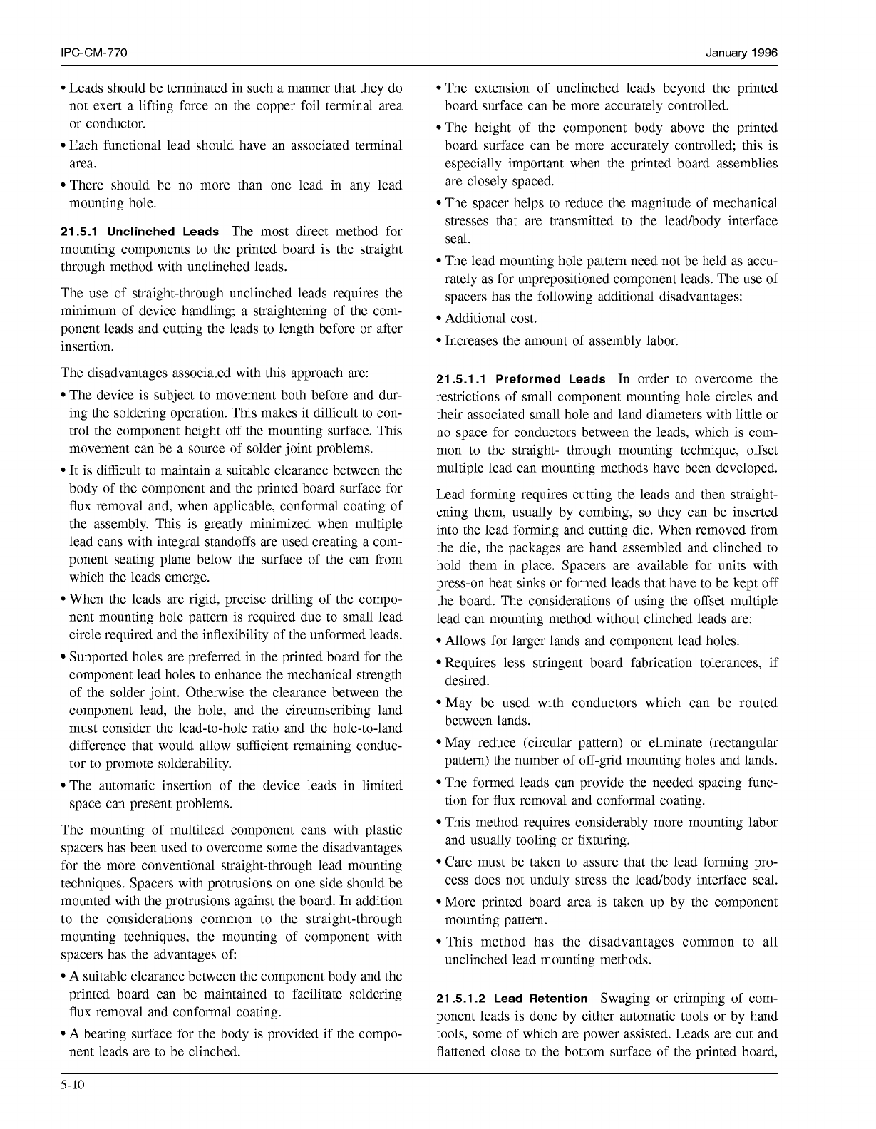
21.4.4 Conforming Material
Conforming sponge-like
material can be used to hold components in place during
wave soldering but has obvious disadvantages of fabrica-
tion, cleaning, removal and frequent replacement. “Bean
bags” or other weighty self- conforming substitutes can be
used.
Web-like materials are available for spraying on the top
surface of the printed board assembly. These set up on
contact and are removable with water or solvents. (See
Figure 21 -2 Component Retention-Deep Solder
Figure
21-3.)
Too heavy an application of the “web-like’’
material can prevent the flow of the solder along the com-
ponent lead and thus result in a lack of a solder fillet on the
component side of the board.
Blister pack, or skin pack, is sometimes used to hold com-
ponents in place during lead trimming and soldering. This
method employs a trans- parent (sometimes bubble) sheet
of plastic.
By means of a blister packing machine a sheet of plastic is
formed over the tops of the components and around edges
of the printed board assembly by the application of heat
and vacuum. Excess plastic is trimmed from the bottom of
the board before lead trimming wave soldering. Plastic is
removed while the board is still warm.
With the blister pack process it is sometimes found that the
plastic material softens and melts during the soldering
5-8
COPYRIGHT Association Connecting Electronics Industries
Licensed by Information Handling Services
COPYRIGHT Association Connecting Electronics Industries
Licensed by Information Handling Services
January
1996
-
IPC-CM-770
Figure 21-3 Conforming Web-like Material
operation and it then adheres to the components leads,
making it difficult to remove.
21.4.5 Wax Stabilizing
Stabilizing is a method by which
long and short component leads are held in position for
automatic lead cutting by a material, not solder, but simi-
larly applied, having adhesive-like holding power. The low
temperature plain wax is applied to the bottom surface by
a deep wave of wax after automatic wave (or spray) flux-
ing and preheating, then through a chiller which hardens
the wax, locking components securely in place for auto-
matic lead cutting which is followed by preheating and
wave soldering. The stabilizing process using flux mixed
with the wax eliminates the separate flux station. Most of
the flux and wax is removed during wave soldering and the
little remaining is removed by either solvent or water
cleaning as appropriate.
21.4.6 Heat Sinking
Excessive exposure time and tem-
perature can cause damage to heat sensitive parts. Thermal
shunts or heat sinks (Figure
21-4)
should be used, as
required, for the protection of heat sensitive parts. They
should be made of a material with good heat conductivity
(e.g. copper) and must be of a size and shape such that
adequate thermal protection and minimum mechanical
interference will be provided during the soldering
operation.
Thermal
Shunt
h(&
b
I
IPC-1-00364
I
Figure 21-4 Thermal Shunt
21.5 Lead Configuration After Assembly
The objectives
of lead termination are to form the lead and electrically
connect it to the conductors in such a manner that the
required circuit continuity is provided through the life of
the equipment regardless of the environments to which the
assembly may be subjected. See Figure
21-5
for the most
frequently used methods.
LEAD AT
i
CLINCHED
LEADS
I
PLATED THROUGH HOLE
I
I
1
NON-PLATED THROUGH HOLE1
I
I
CLINCHED
RIBBON LEAD
LAPPED
PLANAR MOUNTED LEADS
RIBBON AXIAL
LtAD LEAD
STRAIGHT THROUGH
PLATED THROUGH HOLE
I
I
NON~PLATED THROUGH HOLE
-
TERMINALS
IPC-1-00327
Figure 21
-5
Lead Terminations
Leads may be attached to unsupported printed conductor
lands by clinching or straight-through (unclinched) lead
attachment. The attachment should be completed by
soldering.
Component leads should not be used as interfacial
connections.
Component attachment to printed boards should have the
lead or terminal pass through the board and be soldered to
the conductor pattern on the opposite side of the board.
Lead attachment should normally be an option as to
whether clinched or straight-through attachment is used,
with the following restrictions:
Where flat swaged eyelets (unfused) are used, a clinched
lead attachment should be used.
For straight-through attachment the diameter of unsup-
ported holes should not exceed the diameter of the
inserted lead by more than
0.5
mm.
For straight-through lead attachment to supported holes
the inside diameter of the supported hole should not
exceed the diameter of the inserted lead by more than
0.7
mm.
5-9
COPYRIGHT Association Connecting Electronics Industries
Licensed by Information Handling Services
COPYRIGHT Association Connecting Electronics Industries
Licensed by Information Handling Services
IPC-CM-770
Januaty
1996
Leads should be terminated in such a manner that they do
not exert a lifting force on the copper foil terminal area
or conductor.
Each functional lead should have an associated terminal
area.
There should be no more than one lead in any lead
mounting hole.
21.5.1 Unclinched Leads
The most direct method for
mounting components to the printed board is the straight
through method with unclinched leads.
The use of straight-through unclinched leads requires the
minimum of device handling; a straightening of the com-
ponent leads and cutting the leads to length before or after
insertion.
The disadvantages associated with this approach are:
The device is subject to movement both before and dur-
ing the soldering operation. This makes it difficult to con-
trol the component height off the mounting surface. This
movement can be a source of solder joint problems.
It is difficult to maintain a suitable clearance between the
body of the component and the printed board surface for
flux removal and, when applicable, conformal coating of
the assembly. This is greatly minimized when multiple
lead cans with integral standoffs are used creating a com-
ponent seating plane below the surface of the can from
which the leads emerge.
When the leads are rigid, precise drilling of the compo-
nent mounting hole pattern is required due to small lead
circle required and the inflexibility of the unformed leads.
Supported holes are preferred in the printed board for the
component lead holes to enhance the mechanical strength
of the solder joint. Otherwise the clearance between the
component lead, the hole, and the circumscribing land
must consider the lead-to-hole ratio and the hole-to-land
difference that would allow sufficient remaining conduc-
tor to promote solderability.
The automatic insertion of the device leads in limited
space can present problems.
The mounting of multilead component cans with plastic
spacers has been used to overcome some the disadvantages
for the more conventional straight-through lead mounting
techniques. Spacers with protrusions on one side should be
mounted with the protrusions against the board. In addition
to the considerations common to the straight-through
mounting techniques, the mounting of component with
spacers has the advantages
of
A suitable clearance between the component body and the
printed board can be maintained to facilitate soldering
flux removal and conformal coating.
A bearing surface for the body is provided if the compo-
nent leads are to be clinched.
The extension of unclinched leads beyond the printed
board surface can be more accurately controlled.
The height of the component body above the printed
board surface can be more accurately controlled; this is
especially important when the printed board assemblies
are closely spaced.
The spacer helps to reduce the magnitude of mechanical
stresses that are transmitted to the leadhody interface
seal.
The lead mounting hole pattern need not be held as accu-
rately as for unprepositioned component leads. The use of
spacers has the following additional disadvantages:
Additional cost.
Increases the amount of assembly labor.
21.5.1.1 Preformed Leads
In order to overcome the
restrictions of small component mounting hole circles and
their associated small hole and land diameters with little or
no space for conductors between the leads, which is com-
mon to the straight- through mounting technique, offset
multiple lead can mounting methods have been developed.
Lead forming requires cutting the leads and then straight-
ening them, usually by combing,
so
they can be inserted
into the lead forming and cutting die. When removed from
the die, the packages are hand assembled and clinched to
hold them in place. Spacers are available for units with
press-on heat sinks or formed leads that have to be kept off
the board. The considerations of using the offset multiple
lead can mounting method without clinched leads are:
Allows for larger lands and component lead holes.
Requires less stringent board fabrication tolerances, if
desired.
May be used with conductors which can be routed
between lands.
May reduce (circular pattern) or eliminate (rectangular
pattern) the number of off-grid mounting holes and lands.
The formed leads can provide the needed spacing func-
tion for flux removal and conformal coating.
This method requires considerably more mounting labor
and usually tooling or fixturing.
Care must be taken to assure that the lead forming pro-
cess does not unduly stress the leadhody interface seal.
More printed board area is taken up by the component
mounting pattern.
This method has the disadvantages common to all
unclinched lead mounting methods.
21 5.1.2 Lead Retention
Swaging or crimping of com-
ponent leads is done by either automatic tools or by hand
tools, some of which are power assisted. Leads are cut and
flattened close to the bottom surface of the printed board,
5-10
COPYRIGHT Association Connecting Electronics Industries
Licensed by Information Handling Services
COPYRIGHT Association Connecting Electronics Industries
Licensed by Information Handling Services