IPC-CM-770D-1996.pdf - 第35页
January 1996 IPC-CM-770 Printed Wiring Board (Pm) lands for the solder assembly of rectangular chip components should be approximately the same width as the component terminations, Lands that are significantly narrower t…
IPC-CM-770
Januaty
1996
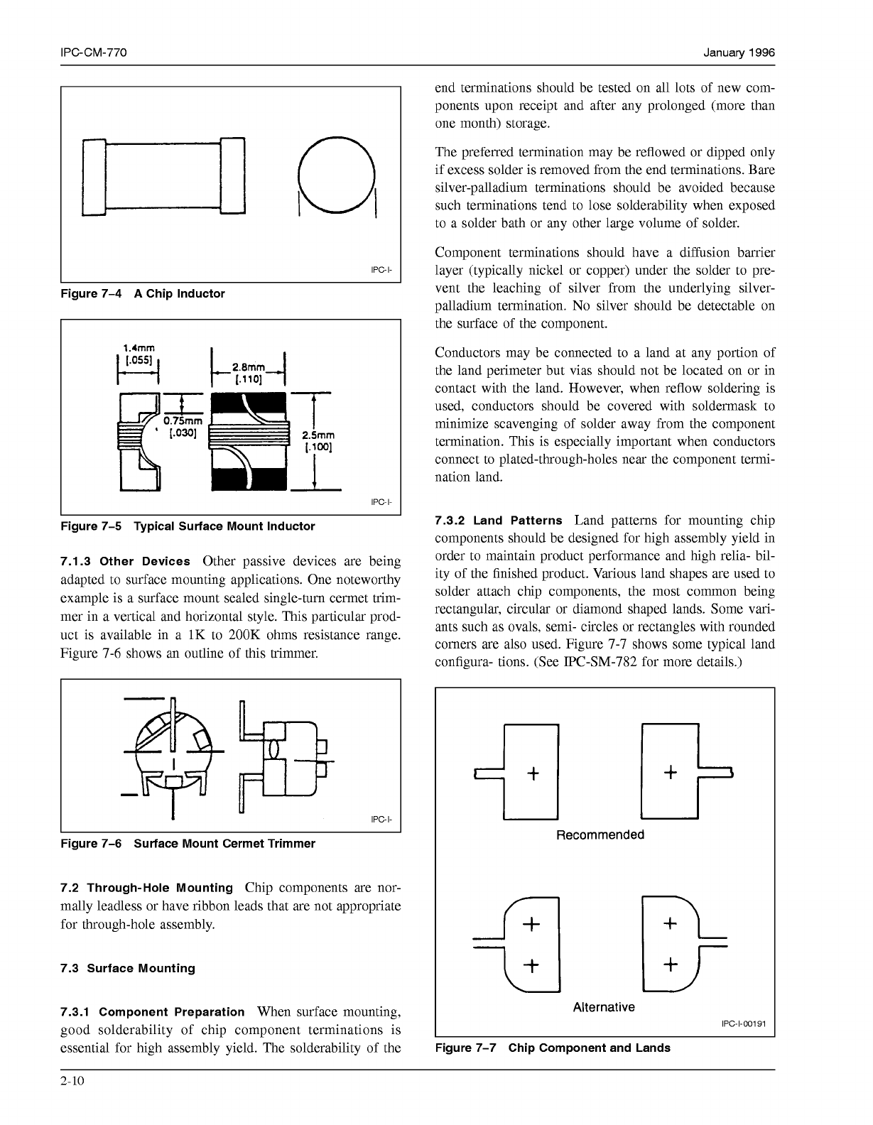
Figure 7-4
A
Chip Inductor
IPC-I-
I
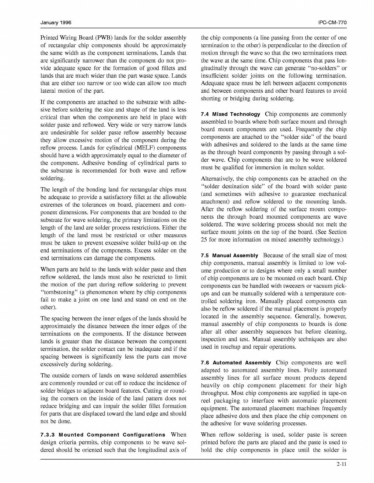
Figure 7-5 Typical Surface Mount Inductor
7.1.3 Other Devices
Other passive devices are being
adapted to surface mounting applications. One noteworthy
example is a surface mount sealed single-turn cermet trim-
mer in a vertical and horizontal style. This particular prod-
uct is available in a 1K to 200K ohms resistance range.
Figure 7-6 shows an outline of this trimmer.
B
I
IPC-I-
L
Figure 7-6 Surface Mount Cermet Trimmer
7.2 Through-Hole Mounting
Chip components are nor-
mally leadless or have ribbon leads that are not appropriate
for through-hole assembly.
7.3 Surface Mounting
7.3.1 Component Preparation
When surface mounting,
good solderability of chip component terminations is
essential for high assembly yield. The solderability of the
end terminations should be tested on all lots of new com-
ponents upon receipt and after any prolonged (more than
one month) storage.
The preferred termination may be reflowed or dipped only
if excess solder is removed from the end terminations. Bare
silver-palladium terminations should be avoided because
such terminations tend to lose solderability when exposed
to a solder bath or any other large volume of solder.
Component terminations should have a diffusion barrier
layer (typically nickel or copper) under the solder to pre-
vent the leaching of silver from the underlying silver-
palladium termination.
No
silver should be detectable on
the surface of the component.
Conductors may be connected to a land at any portion of
the land perimeter but vias should not be located on or in
contact with the land. However, when reflow soldering is
used, conductors should be covered with soldermask to
minimize scavenging of solder away from the component
termination. This is especially important when conductors
connect to plated-through-holes near the component termi-
nation land.
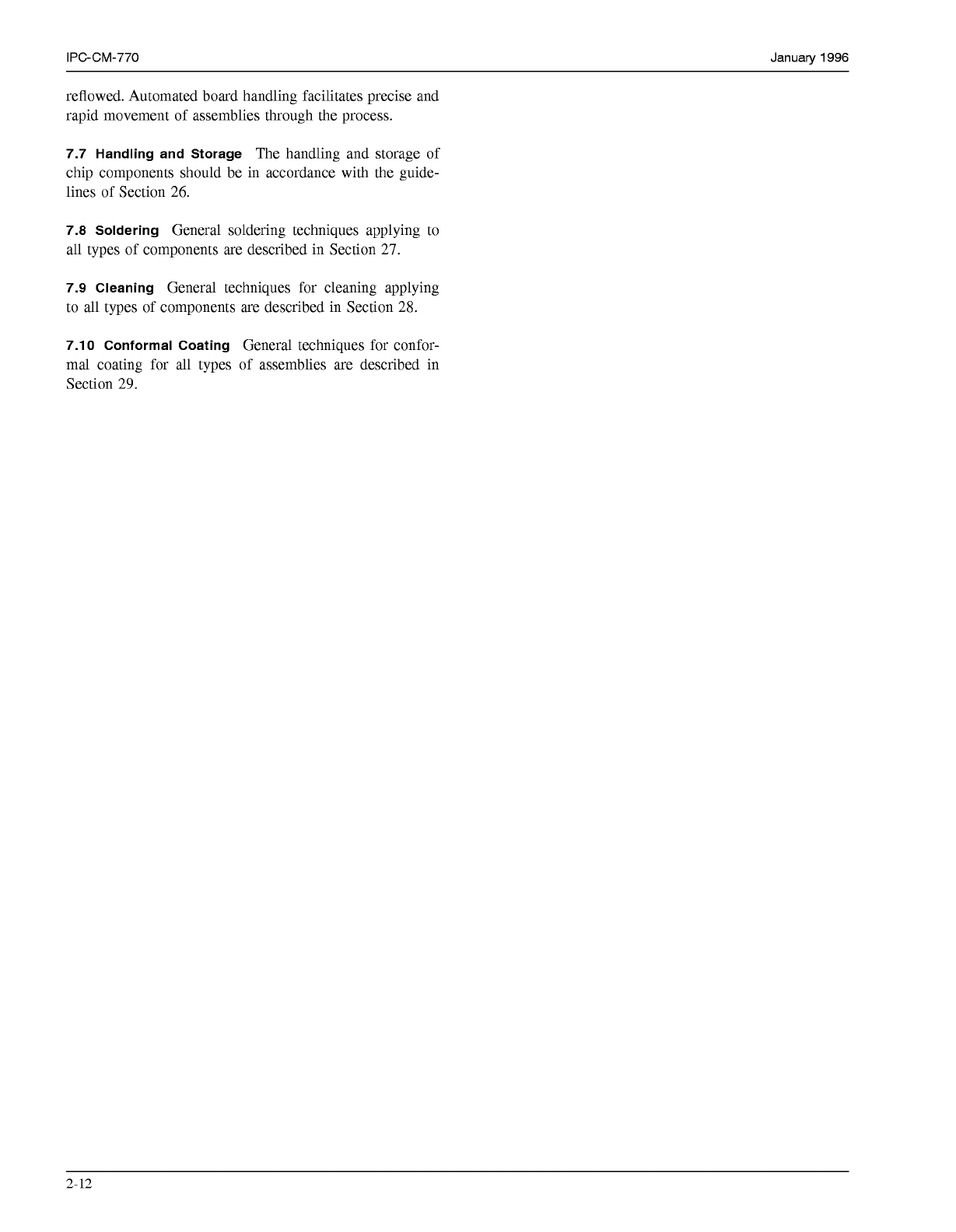
7.3.2 Land Patterns
Land patterns for mounting chip
components should be designed for high assembly yield in
order to maintain product performance and high relia- bil-
ity of the finished product. Various land shapes are used to
solder attach chip components, the most common being
rectangular, circular or diamond shaped lands. Some vari-
ants such as ovals, semi- circles or rectangles with rounded
comers are also used. Figure 7-7 shows some typical land
configura- tions. (See PC-SM-782 for more details.)
Recommended
Alternative
IPC-1-00191
Figure 7-7 Chip Component and Lands
2-10
COPYRIGHT Association Connecting Electronics Industries
Licensed by Information Handling Services
COPYRIGHT Association Connecting Electronics Industries
Licensed by Information Handling Services
January
1996
IPC-CM-770
Printed Wiring Board
(Pm)
lands for the solder assembly
of rectangular chip components should be approximately
the same width as the component terminations, Lands that
are significantly narrower than the component do not pro-
vide adequate space for the formation of good fillets and
lands that are much wider than the part waste space. Lands
that are either too narrow or too wide can allow too much
lateral motion of the part.
If the components are attached to the substrate with adhe-
sive before soldering the size and shape of the land is less
critical than when the components are held in place with
solder paste and reflowed. Very wide or very narrow lands
are undesirable for solder paste reflow assembly because
they allow excessive motion of the component during the
reflow process. Lands for cylindrical (MELF) components
should have a width approximately equal to the diameter of
the component. Adhesive bonding of cylindrical parts to
the substrate is recommended for both wave and reflow
soldering.
The length of the bonding land for rectangular chips must
be adequate to provide a satisfactory fillet at the allowable
extremes of the tolerances on board, placement and com-
ponent dimensions. For components that are bonded to the
substrate for wave soldering, the primary limitations on the
length of the land are solder process restrictions. Either the
length of the land must be restricted or other measures
must be taken to prevent excessive solder build-up on the
end terminations of the components. Excess solder on the
end terminations can damage the components.
When parts are held to the lands with solder paste and then
reflow soldered, the lands must also be restricted to limit
the motion of the part during reflow soldering to prevent
“tombstoning” (a phenomenon where by chip components
fail to make a joint on one land and stand on end on the
other).
The spacing between the inner edges of the lands should be
approximately the distance between the inner edges of the
terminations on the components. If the distance between
lands is greater than the distance between the component
termination, the solder contact can be inadequate and if the
spacing between is significantly less the parts can move
excessively during soldering.
The outside comers of lands on wave soldered assemblies
are commonly rounded or cut
off
to reduce the incidence of
solder bridges to adjacent board features. Cutting or round-
ing the comers on the inside of the land pattern does not
reduce bridging and can impair the solder fillet formation
for parts that are displaced toward the land edge and should
not be done.
7.3.3 Mounted Component Configurations
When
design criteria permits, chip components to be wave sol-
dered should be oriented such that the longitudinal axis of
the chip components (a line passing from the center of one
termination to the other) is perpendicular to the direction of
motion through the wave
so
that the two terminations meet
the wave at the same time. Chip components that pass lon-
gitudinally through the wave can generate “no-solders’’ or
insufficient solder joints on the following termination.
Adequate space must be left between adjacent components
and between components and other board features to avoid
shorting or bridging during soldering.
7.4 Mixed Technology
Chip components are commonly
assembled to boards where both surface mount and through
board mount components are used. Frequently the chip
components are attached to the “solder side” of the board
with adhesives and soldered to the lands at the same time
as the through board components by passing through a sol-
der wave. Chip components that are to be wave soldered
must be qualified for immersion in molten solder.
Alternatively, the chip components can be attached on the
“solder destination side” of the board with solder paste
(and sometimes with adhesive to guarantee mechanical
attachment) and reflow soldered to the mounting lands.
After the reflow soldering of the surface mount compo-
nents the through board mounted components are wave
soldered. The wave soldering process should not melt the
surface mount joints on the top of the board. (See Section
25
for more information on mixed assembly technology.)
7.5 Manual Assembly
Because of the small size of most
chip components, manual assembly is limited to low vol-
ume production or to designs where only a small number
of chip components are to be mounted on each board. Chip
components can be handled with tweezers or vacuum pick-
ups and can be manually soldered with a temperature con-
trolled soldering iron. Manually placed components can
also be reflow soldered if the manual placement is properly
located in the assembly sequence. Generally, however,
manual assembly of chip components to boards is done
after all other assembly sequences but before cleaning,
inspection and test. Manual assembly techniques are also
used in touchup and repair operations.
7.6 Automated Assembly
Chip components are well
adapted to automated assembly lines. Fully automated
assembly lines for all surface mount products depend
heavily on chip component placement for their high
throughput. Most chip components are supplied in tape-on
reel packaging to interface with automatic placement
equipment. The automated placement machines frequently
place adhesive dots and then place the chip component on
the adhesive for wave soldering processes.
When reflow soldering is used, solder paste is screen
printed before the parts are placed and the paste is used to
hold the chip components in place until the solder is
2-11
COPYRIGHT Association Connecting Electronics Industries
Licensed by Information Handling Services
COPYRIGHT Association Connecting Electronics Industries
Licensed by Information Handling Services
IPC-CM-770
Januaty
1996
reflowed. Automated board handling facilitates precise and
rapid movement of assemblies through the process.
7.7
Handling and Storage
The handling and storage
of
chip components should be in accordance with the guide-
lines of Section
26.
7.8
Soldering
General soldering techniques applying to
all types of components are described in Section
27.
7.9
Cleaning
General techniques for cleaning applying
to all types of components are described in Section
28.
7.10
Conformal Coating
General techniques for confor-
mal coating for all types of assemblies are described in
Section
29.
2-12
COPYRIGHT Association Connecting Electronics Industries
Licensed by Information Handling Services
COPYRIGHT Association Connecting Electronics Industries
Licensed by Information Handling Services