IPC-CM-770D-1996.pdf - 第58页
IPC-CM-770 Januaty 1996 make adequate contact with substrate solder lands. Flatness of the substrate is also of concern and needs to be con- trolled. 12.3.2 Land Patterns The land patterns used with chip carriers fall in…
January
1996
IPC-CM-770
IPC-I-
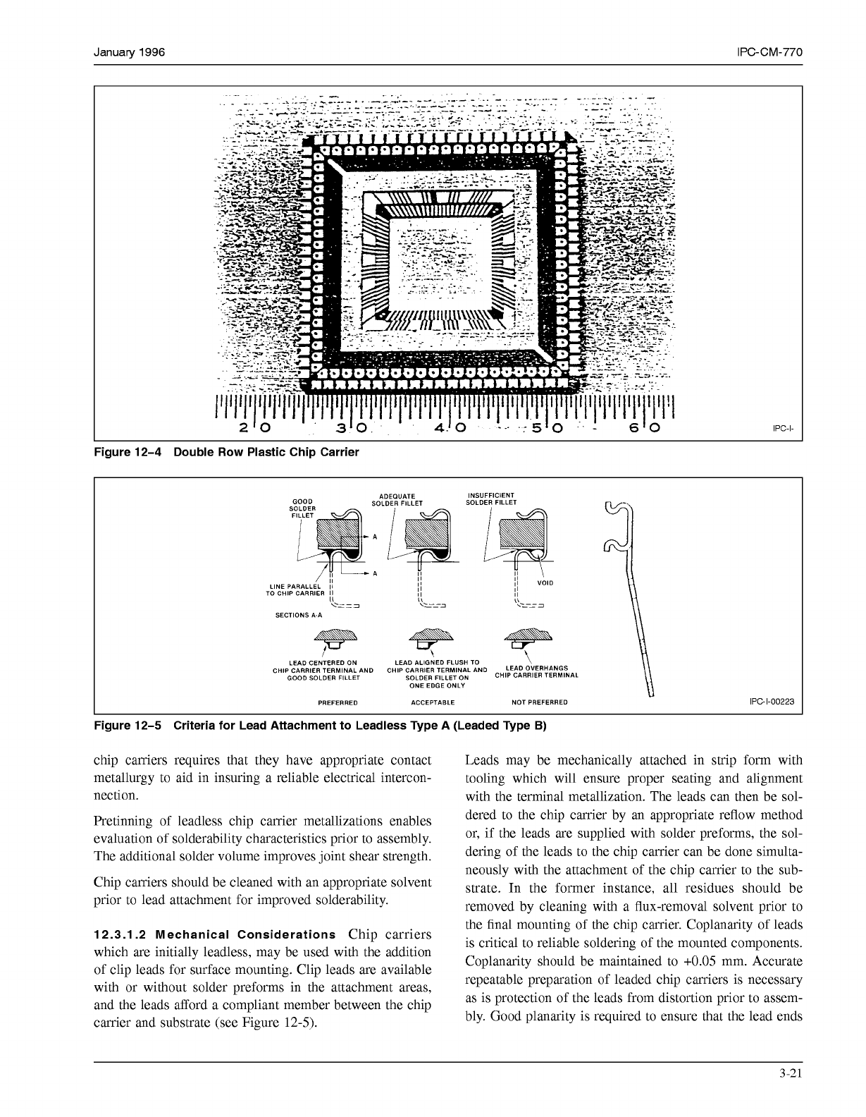
Figure 12-4 Double
Row
Plastic Chip Carrier
ADEQUATE
GOOD SOLDER FILLET
A
LINE PARALLEL
Il
TO CHIP CARRIER
II
SOLDER FILLET
INSUFFICIENT
LEAD CENTERED ON
GOOD SOLDER FILLET
CHIP CARRIER TERMINAL AND CHIP CARRIER TERMINAL AND
LEAD
OVERHANGS
LEAD ALIGNED FLUSH
TO
\
SOLDER
oN
CHIP CARRIER TERMINAL
\\
ONE EDGE ONLY
PREFERRED ACCEPTABLE NOT PREFERRED
IPC-1-00223
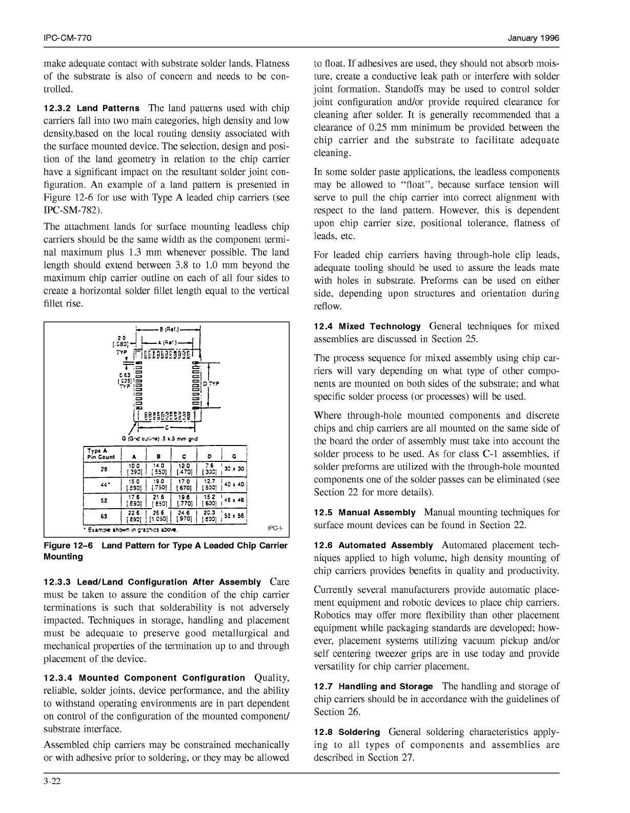
Figure 12-5 Criteria for Lead Attachment to Leadless Type A (Leaded Type
B)
chip carriers requires that they have appropriate contact
metallurgy to aid in insuring a reliable electrical intercon-
nection.
Pretinning of leadless chip carrier metallizations enables
evaluation of solderability characteristics prior to assembly.
The additional solder volume improves joint shear strength.
Chip carriers should be cleaned with an appropriate solvent
prior to lead attachment for improved solderability.
12.3.1.2 Mechanical Considerations
Chip carriers
which are initially leadless, may be used with the addition
of clip leads for surface mounting. Clip leads are available
with or without solder preforms in the attachment areas,
and the leads afford a compliant member between the chip
carrier and substrate (see Figure
12-5).
Leads may be mechanically attached in strip form with
tooling which will ensure proper seating and alignment
with the terminal metallization. The leads can then be sol-
dered to the chip carrier by an appropriate reflow method
or, if the leads are supplied with solder preforms, the sol-
dering of the leads to the chip carrier can be done simulta-
neously with the attachment of the chip carrier to the sub-
strate. In the former instance, all residues should be
removed by cleaning with a flux-removal solvent prior to
the final mounting of the chip carrier. Coplanarity of leads
is critical to reliable soldering of the mounted components.
Coplanarity should be maintained to
+0.05
mm. Accurate
repeatable preparation of leaded chip carriers is necessary
as is protection of the leads from distortion prior to assem-
bly. Good planarity is required to ensure that the lead ends
3-21
COPYRIGHT Association Connecting Electronics Industries
Licensed by Information Handling Services
COPYRIGHT Association Connecting Electronics Industries
Licensed by Information Handling Services
IPC-CM-770
Januaty
1996
make adequate contact with substrate solder lands. Flatness
of the substrate is also of concern and needs to be con-
trolled.
12.3.2 Land Patterns
The land patterns used with chip
carriers fall into two main categories, high density and low
density,based on the local routing density associated with
the surface mounted device. The selection, design and posi-
tion of the land geometry in relation to the chip carrier
have a significant impact on the resultant solder joint con-
figuration. An example of a land pattern is presented in
Figure 12-6 for use with Type A leaded chip carriers (see
IPC-SM-782).
The attachment lands for surface mounting leadless chip
carriers should be the same width as the component termi-
nal maximum plus 1.3 mm whenever possible. The land
length should extend between 3.8 to
1.0
mm beyond the
maximum chip carrier outline on each of all four sides to
create a horizontal solder fillet length equal to the vertical
fillet rise.
IPC-I-
L
Figure 12-6 Land Pattern for Type A Leaded Chip Carrier
Mounting
12.3.3 LeadlLand Configuration After Assembly
Care
must be taken to assure the condition of the chip carrier
terminations is such that solderability is not adversely
impacted. Techniques in storage, handling and placement
must be adequate to preserve good metallurgical and
mechanical properties of the termination up to and through
placement of the device.
12.3.4 Mounted Component Configuration
Quality,
reliable, solder joints, device performance, and the ability
to withstand operating environments are in part dependent
on control of the configuration of the mounted component/
substrate interface.
Assembled chip carriers may be constrained mechanically
or with adhesive prior to soldering, or they may be allowed
to float.
If
adhesives are used, they should not absorb mois-
ture, create a conductive leak path or interfere with solder
joint formation. Standoffs may be used to control solder
joint configuration and/or provide required clearance for
cleaning after solder. It is generally recommended that a
clearance of 0.25 mm minimum be provided between the
chip carrier and the substrate to facilitate adequate
cleaning.
In some solder paste applications, the leadless components
may be allowed to “float”, because surface tension will
serve to pull the chip carrier into correct alignment with
respect to the land pattern. However, this is dependent
upon chip carrier size, positional tolerance, flatness of
leads, etc.
For leaded chip carriers having through-hole clip leads,
adequate tooling should be used to assure the leads mate
with holes in substrate. Preforms can be used on either
side, depending upon structures and orientation during
reflow.
12.4 Mixed Technology
General techniques for mixed
assemblies are discussed in Section 25.
The process sequence for mixed assembly using chip car-
riers will vary depending on what type of other compo-
nents are mounted on both sides of the substrate; and what
specific solder process (or processes) will be used.
Where through-hole mounted components and discrete
chips and chip carriers are all mounted on the same side of
the board the order of assembly must take into account the
solder process to be used. As for class C-1 assemblies, if
solder preforms are utilized with the through-hole mounted
components one of the solder passes can be eliminated (see
Section 22 for more details).
12.5 Manual Assembly
Manual mounting techniques for
surface mount devices can be found in Section 22.
12.6 Automated Assembly
Automated placement tech-
niques applied to high volume, high density mounting of
chip carriers provides benefits in quality and productivity.
Currently several manufacturers provide automatic place-
ment equipment and robotic devices to place chip carriers.
Robotics may offer more flexibility than other placement
equipment while packaging standards are developed; how-
ever, placement systems utilizing vacuum pickup and/or
self centering tweezer grips are in use today and provide
versatility for chip carrier placement.
12.7 Handling and Storage
The handling and storage of
chip carriers should be in accordance with the guidelines of
Section 26.
12.8 Soldering
General soldering characteristics apply-
ing to all types of components and assemblies are
described in Section 27.
3
-22
COPYRIGHT Association Connecting Electronics Industries
Licensed by Information Handling Services
COPYRIGHT Association Connecting Electronics Industries
Licensed by Information Handling Services
January
1996
IPC-CM-770
12.9 Cleaning
General techniques for cleaning applying
to all types of components are described in Section 28.
Because of generally smaller spacing between leads,
smaller clearances between substrate and the component
body, and large area beneath the devices, chip carriers
present a more difficult cleaning situation than through-
hole mounted devices. Clearance under the package should
be adequate to facilitate an effective cleaning operation.
Some surface mounting soldering processes result in
exposing the fluxes to high heat for longer and repeated
periods of time than experienced with through-hole compo-
nent soldering. This can lead to a more stable flux residue
making the cleaning more difficult. There is generally less
flux residue associated with chip carriers, but it is concen-
trated in smaller crevices under and between close spaced
devices.
Techniques using azeotropic solvents, aqueous cleaning
with detergents, as well as combinations of aqueous and
solvent cleaning process have been successfully applied.
12.10 Conformal Coating
General techniques for con-
formal coating for all types of assemblies are described in
Section 29.
13.0 AREA ARRAY COMPONENTS
The advent of very large scale integration (VLSI) and very
high speed integrated circuit (VHSIC) has brought a need
for very high pin count packages with lead symmetry and
methods to reliably assemble them onto circuit boards.
Grid arrays are pinned or leadless carriers with I/O contacts
that populate one surface of the package on a
0.100
inch
(eventually
0.050
inch) grid. The use of a solid grid neces-
sitates placing the die cavity on the side opposite the
Il0
contacts.
A
double or multiple concentric row grid permits
having die cavity and
Il0
contacts on the same side with
an optional heat sink on the opposite side.
13.1 Pin Grid Array Components
13.1.1 Port Types
The pin grid array package is the
package designed for high pin out ICs for through-hole
mounting because of its space efficiency and compatibility
with existing DIP facilities.
The main advantage of the pin-array is to avoid the
Il0
limitations of peripherally terminated packages such as
LCC at the same time providing terminal separations of
100-mil centerlines.
As
such it can be readily installed into
a conventional printed board and also wave soldered.
Offset disadvantages which have to be weighed:
Inspection of solder joints
Impedance limitations
Removal and replacement
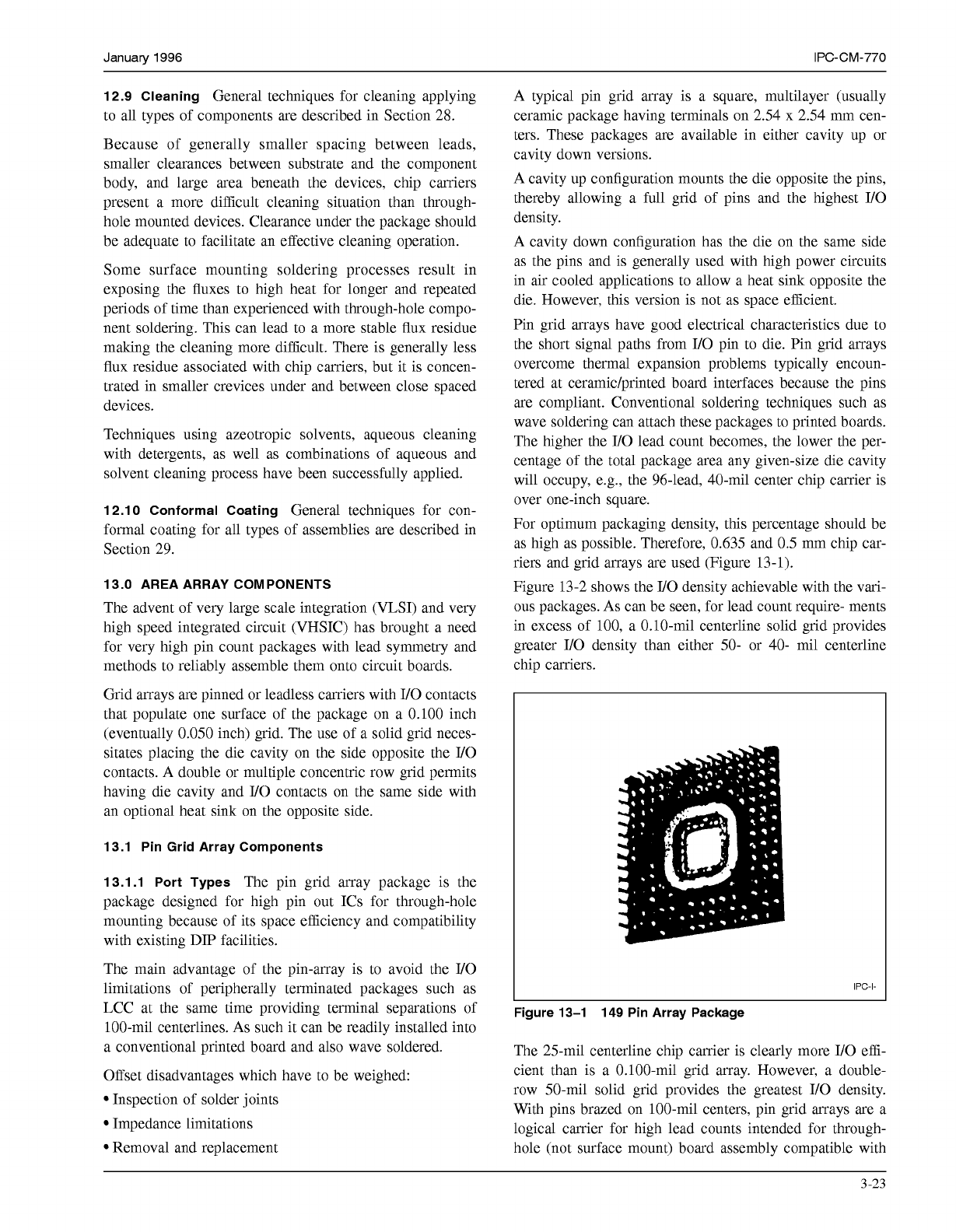
A
typical pin grid array is a square, multilayer (usually
ceramic package having terminals on 2.54 x 2.54 mm cen-
ters. These packages are available in either cavity up or
cavity down versions.
A
cavity up configuration mounts the die opposite the pins,
thereby allowing a full grid of pins and the highest I/O
density.
A
cavity down configuration has the die on the same side
as the pins and is generally used with high power circuits
in air cooled applications to allow a heat sink opposite the
die. However, this version is not as space efficient.
Pin grid arrays have good electrical characteristics due to
the short signal paths from I/O pin to die. Pin grid arrays
overcome thermal expansion problems typically encoun-
tered at ceramic/printed board interfaces because the pins
are compliant. Conventional soldering techniques such as
wave soldering can attach these packages to printed boards.
The higher the I/O lead count becomes, the lower the per-
centage of the total package area any given-size die cavity
will occupy, e.g., the 96-lead, 40-mil center chip carrier is
over one-inch square.
For optimum packaging density, this percentage should be
as high as possible. Therefore, 0.635 and
0.5
mm chip car-
riers and grid arrays are used (Figure 13-1).
Figure 13-2 shows the
Il0
density achievable with the vari-
ous packages.
As
can be seen, for lead count require- ments
in excess of
100,
a 0.10-mil centerline solid grid provides
greater I/O density than either
50-
or 40- mil centerline
chip carriers.
IPC-I-
Figure 13-1 149 Pin Array Package
The 25-mil centerline chip carrier is clearly more I/O effi-
cient than is a 0.100-mil grid array. However, a double-
row 50-mil solid grid provides the greatest I/O density.
With pins brazed on 100-mil centers, pin grid arrays are a
logical carrier for high lead counts intended for through-
hole (not surface mount) board assembly compatible with
3-23
COPYRIGHT Association Connecting Electronics Industries
Licensed by Information Handling Services
COPYRIGHT Association Connecting Electronics Industries
Licensed by Information Handling Services