IPC-CM-770D-1996.pdf - 第90页
IPC-CM-770 Januaty 1996 I IPC-1-00268 I Figure 17-1 6 Terminal Installation, Single-Sided Board, Soldered on Flared Flange Side IPC-1-00269 I L Figure 17-17 Installation of Terminal in Plated-through Hole r-"" …
January
1996
IPC-CM-770
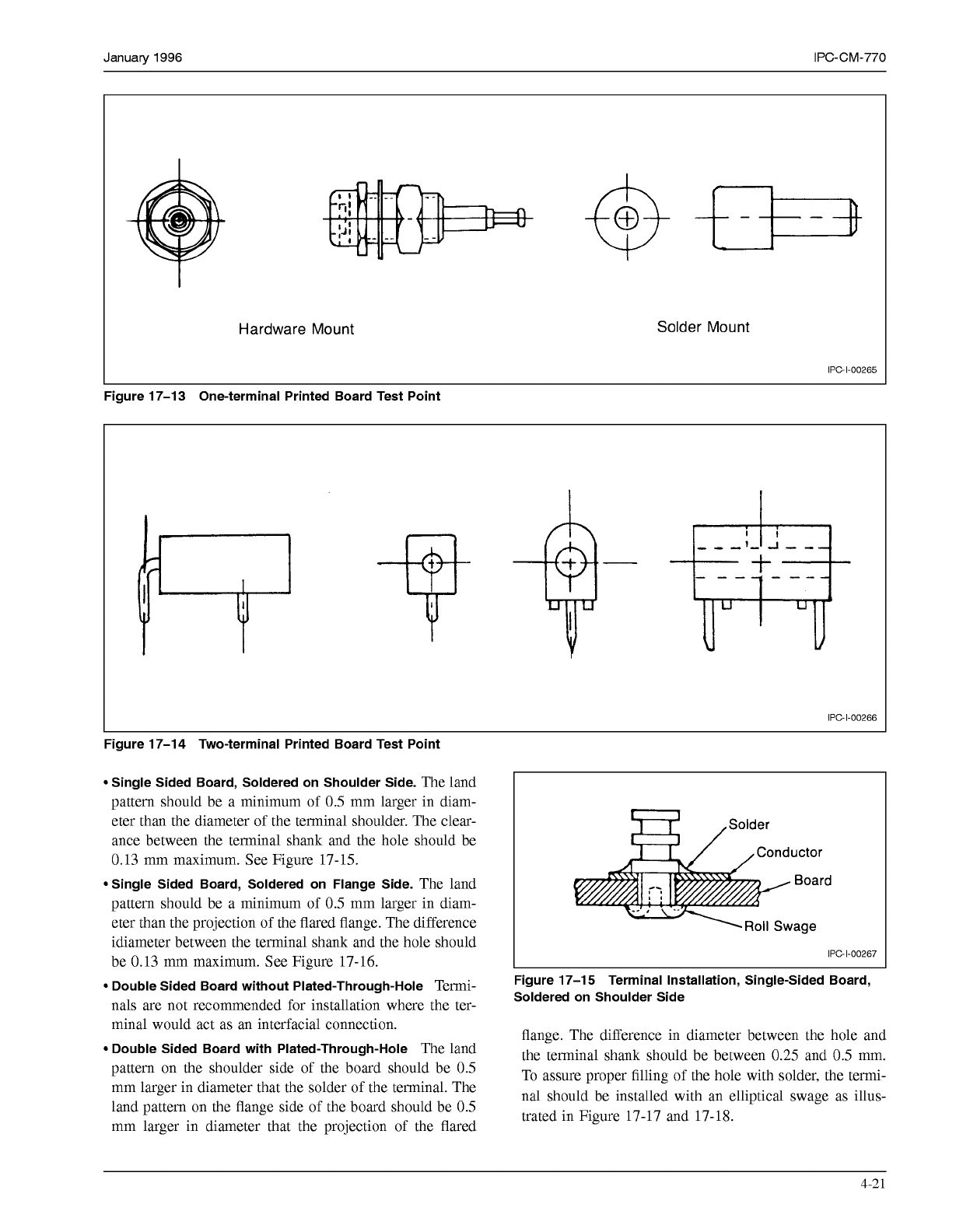
Hardware Mount
Solder Mount
IPC-1-00265
Figure 17-13 One-terminal Printed Board Test Point
IPC-1-00266
Figure 17-1
4
Two-terminal Printed Board Test Point
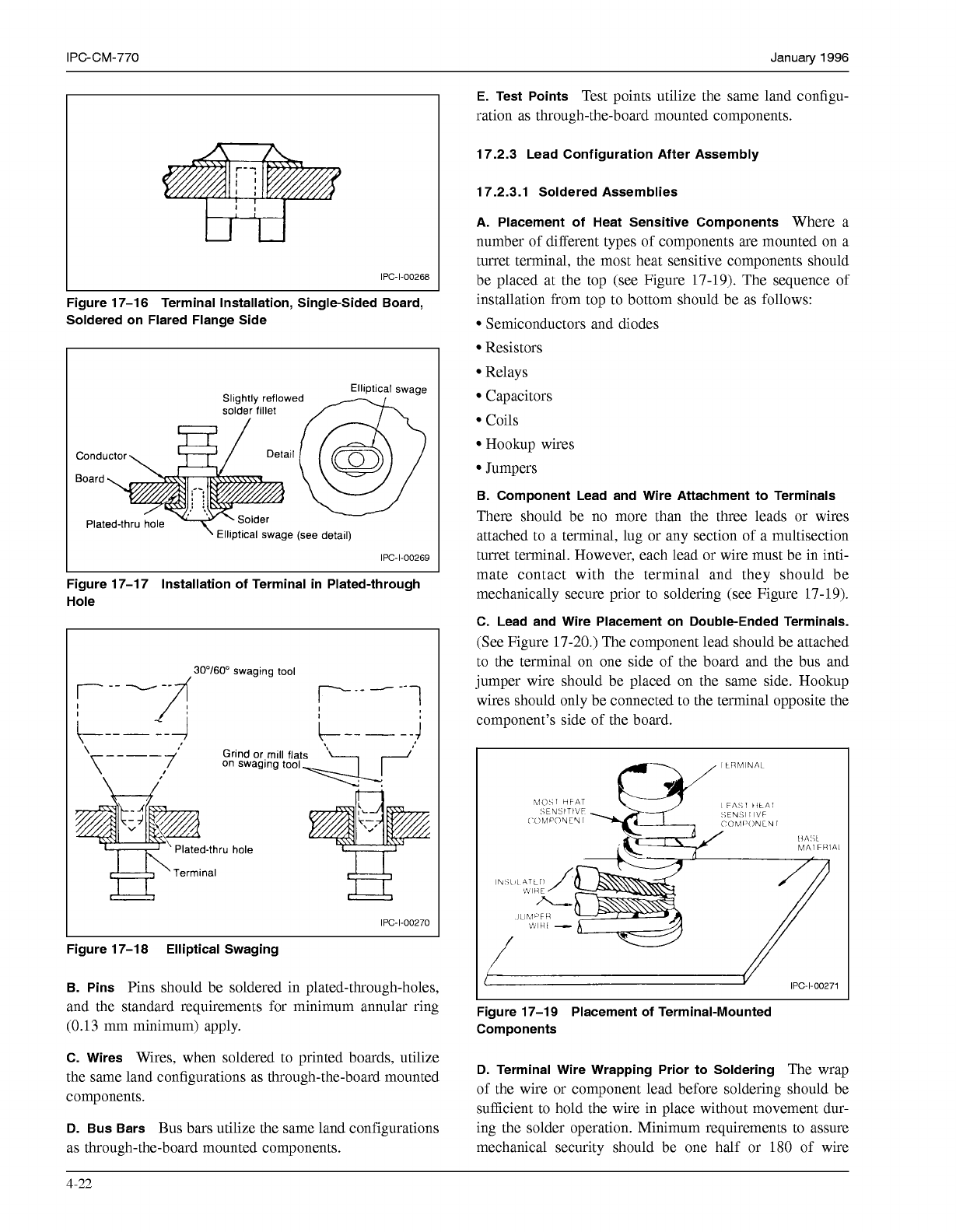
Single Sided Board, Soldered on Shoulder Side.
The land
pattern should be a minimum of
0.5
mm larger in diam-
eter than the diameter of the terminal shoulder. The clear-
ance between the terminal shank and the hole should be
0.13
mm maximum. See Figure
17-15.
Single Sided Board, Soldered on Flange Side.
The land
pattern should be a minimum of
0.5
mm larger in diam-
eter than the projection of the flared flange. The difference
idiameter between the terminal shank and the hole should
be
0.13
mm maximum. See Figure
17-16.
Double Sided Board without Plated-Through-Hole
Termi-
nals are not recommended for installation where the ter-
minal would act as an interfacial connection.
Double Sided Board with Plated-Through-Hole
The land
pattern on the shoulder side of the board should be
0.5
mm larger in diameter that the solder of the terminal. The
land pattern on the flange side of the board should be
0.5
mm larger in diameter that the projection of the flared
I
IPC-1-00267
Figure 17-15 Terminal Installation, Single-Sided Board,
Soldered on Shoulder Side
flange. The difference in diameter between the hole and
the terminal shank should be between
0.25
and
0.5
mm.
To assure proper filling of the hole with solder, the termi-
nal should be installed with an elliptical swage as illus-
trated in Figure
17-17
and
17-18.
4-21
COPYRIGHT Association Connecting Electronics Industries
Licensed by Information Handling Services
COPYRIGHT Association Connecting Electronics Industries
Licensed by Information Handling Services
IPC-CM-770
Januaty
1996
I
IPC-1-00268
I
Figure 17-1
6
Terminal Installation, Single-Sided Board,
Soldered on Flared Flange Side
IPC-1-00269
I
L
Figure 17-17 Installation of Terminal in Plated-through
Hole
r-""
30"160"
swaging
tool
r--
-
"1
I
\
\"",I
on swagmg
tool
Grind or.mlll flats
I
Plated-thru
hole
IPC-I-O0270
L
Figure 17-1
8
Elliptical Swaging
B. Pins
Pins should be soldered in plated-through-holes,
and the standard requirements for minimum annular ring
(0.13
mm minimum) apply.
C. Wires
Wires, when soldered to printed boards, utilize
the same land configurations as through-the-board mounted
components.
D. Bus Bars
Bus bars utilize the same land configurations
as through-the-board mounted components.
E. Test Points
Test points utilize the same land configu-
ration as through-the-board mounted components.
17.2.3 Lead Configuration After Assembly
17.2.3.1 Soldered Assemblies
A. Placement of Heat Sensitive Components
Where a
number of different types of components are mounted on a
turret terminal, the most heat sensitive components should
be placed at the top (see Figure 17-19). The sequence of
installation from top to bottom should be as follows:
Semiconductors and diodes
Resistors
Relays
Capacitors
Coils
Hookup wires
Jumpers
B. Component Lead and Wire Attachment to Terminals
There should be no more than the three leads or wires
attached to a terminal, lug or any section of a multisection
turret terminal. However, each lead or wire must be in inti-
mate contact with the terminal and they should be
mechanically secure prior to soldering (see Figure 17-19).
C. Lead and Wire Placement on Double-Ended Terminals.
(See Figure 17-20.) The component lead should be attached
to the terminal on one side of the board and the bus and
jumper wire should be placed on the same side. Hookup
wires should only be connected to the terminal opposite the
component's side of the board.
V
IPC-I-O0271
Figure 17-19 Placement of Terminal-Mounted
Components
D. Terminal Wire Wrapping Prior to Soldering
The wrap
of the wire or component lead before soldering should be
sufficient to hold the wire in place without movement dur-
ing the solder operation. Minimum requirements to assure
mechanical security should be one half or
180
of wire
4-22
COPYRIGHT Association Connecting Electronics Industries
Licensed by Information Handling Services
COPYRIGHT Association Connecting Electronics Industries
Licensed by Information Handling Services
January
1996
IPC-CM-770
wrap. The maximum wire wrap should not overlap (see
Figure 17-21).
I I
W
Hook-up
Figure 17-20 Double-ended Terminal
(a)
Mlnlmum
Wrap
I
Blfurcated
(SPllt)
lug
Turret
lug
I
(b)
Maxlmum Wrap
Hook
lug
\
IPC
-1-00095
L
Figure 17-21 Terminal Wrap Prior to Soldering
E.
Jumper Wires
Component leads should not be used for
the purpose of jumper wires, bus wires or for interfacial
connections on printed boards. Jumper wires should be as
direct and as short as possible, without being taut, and
should not be routed over or under other components.
Where continuity between the two sides of a printed board
is desired, a short piece of unsleeved bus wire is used
either in a “C” or “Z” shape to conform to pattern
restrictions.
F. Point to Point Connections
The following rules should
be adhered to in selecting point to point jumper wires.
Bus wire over
1
inch long should be sleeved, and secured
to the board at one- inch intervals.
Bus wire crossing conductors should be sleeved.
Bend radii will conform to normal component bend
requirements.
The shortest route will be used unless design consider-
ations dictate otherwise.
Sleeving will be of sufficient length that slippage to either
end will not result in a gap between the insulation and
solder joint or bend of more than 3.2 mm. Sleeving
should not show damage caused by the soldering opera-
tion. (See Figure 17-22.)
3.2 mm 1.5 mm
-
,
[0.125”] max.
,
[0.060”] min
-
-
(al
Supported
Holes
-~
PTH
or
Eyelet
1.5 mm[0.060”] min.
r3i; mm [0.125”] max
Terrnlnal
post
i-
v///////a///A
(b)
Termlnals
IPC-1-00272
Figure 17-22 Methods
of
Mounting Jumpers
G. Jumper Wires or Leads Crossing Conductors
All
jumper wires crossing printed wiring conductor or conduc-
tors should be insulated with insulation sleeving. Compo-
nent leads should be insulated if they are within 1.27 mm
of the conductor surface, or over 9.52 mm in length from
the component body to bend radius. Large, supported, or
anchored components may not fall in this category.
H.
Insulation Clearance
The clearance between the end of
the insulation and the solder of the connection should be as
follows:
Minimum Clearance
The insulation should not be
embedded in the solder connection or touch the terminal.
The contour of the conductor should not be obscured at
the termination end of the insulation.
Maximum Clearance
Clearance should be less than two
wire diameters including insulation, or
0.15
mm, which-
ever is larger, but should not permit shorting to adjacent
conductors or terminals.
1.
Wire Bending Tools
Wire bending tools should be used
to form component lead and wires when preforming is
required. Round nose or protected long nose pliers may be
used as a bending tool. Bending tools, manual or auto-
matic, should not nick the wire. Other deformation should
not reduce the wire cross sectional area more than ten
percent.
17.2.3.2 Solderless (Wire) Wrap Assemblies
A. Wire Wrapping Guidelines
The following material is
provided to explain various types of solderless wrapped
connections. Figure 17-23 shows the common terminology
of this type of interconnection.
Conventional solderless wrapped connection consists of a
helix of continuous, solid, uninsulated wire tightly
wrapped around a suitable wrapost to produce a mechani-
cally and electrically stable connection (see Figure
4-23
COPYRIGHT Association Connecting Electronics Industries
Licensed by Information Handling Services
COPYRIGHT Association Connecting Electronics Industries
Licensed by Information Handling Services