IPC-CM-770D-1996.pdf - 第130页
IPC-CM-770 Januaty 1996 Straight for 1 D but not less than 0.8mm " Flush to 0.635mm [0.25] Max Cqonductor IPC-1-00363 L Figure 25-2 Component Modifications for Surface Mounting Applications chip components between t…
January
1996
IPC-CM-770
and can be stored at room temperature for up to two years.
After encapsulation, the materials are dried to drive off the
solvent vehicle.
25.0 INTERMIXED TECHNOLOGY
Sections 21, 22, 23 and 24 cover the principles of compo-
nent mounting -where components are mounted through-
the-board and components are surface mounted. Intermix-
ing of the techniques on the same electronic assembly adds
an additional dimension to the aspects of component
mounting. Although the techniques used for through-hole
and surface mounting in intermixed assemblies are similar
to the approach used in “all the same type of mounting”
assemblies, there are many additional concerns facing the
assembler of printed boards who uses both technologies in
the same assembly.
25.1 General Considerations
Because of the dual or
multistep component mounting operation, the designer of
intermixed assemblies must take into account all of the
fabrication and assembly steps necessary to complete the
electronic assembly. These concerns that take place during
the design cycle include:
A. Component Types
B.
The Assembly Processes Used
Single-sided assembly
Double-side assembly
Component securing
C. Joining Techniques
Single-sided joining techniques
Double-sided joining techniques
Care required for heat-sensitive components
Handling of unsealed components
D. Sequence of Events
The last item on the list shown above is usually never con-
sidered during the design cycle; however, in intermixed
assemblies, if the sequencing of component mounting is
not taken into account, components will interfere with one
another or will be removed during a second mounting step.
25.1.1 LeadlLand Relationships
Hole and land require-
ments for intermixed assembly are identical to those
requirements already stipulated in through-the-board and
surface mounted land pattern configurations.
No
special
requirements are necessary and implementation of the
proper land pattern into the design will provide the appro-
priate solder joint after placement.
25.1.2 Component Preparation
All lead extension and
forming requirements on parts to be mounted on printed
board structures are identical to the techniques described
for through-the-board and surface mount component
mounting and positioning.
One major difference to be acknowledged is that some
individuals have chosen to reduce the number of compo-
nent mounting and attachment sequences by taking compo-
nents designed for through- the-board mounting and con-
verting them to surface mount parts; or parts that are
designed for surface mounting are converted to through-
the-board mounted parts.
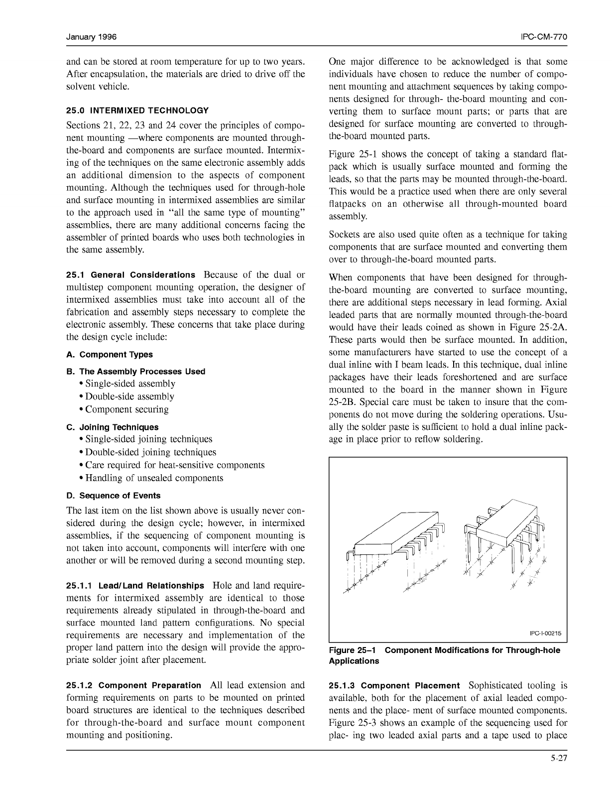
Figure 25-1 shows the concept of taking a standard flat-
pack which is usually surface mounted and forming the
leads,
so
that the parts may be mounted through-the-board.
This would be a practice used when there are only several
flatpacks on an otherwise all through-mounted board
assembly.
Sockets are also used quite often as a technique for taking
components that are surface mounted and converting them
over to through-the-board mounted parts.
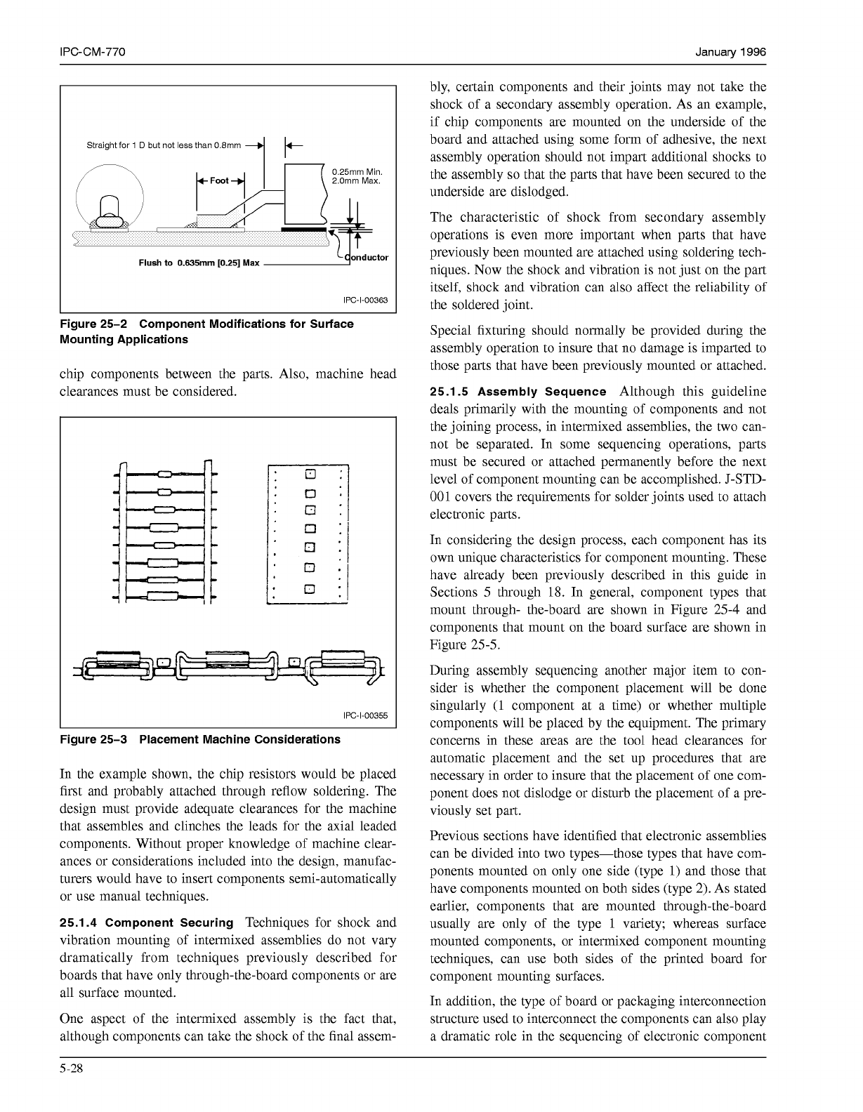
When components that have been designed for through-
the-board mounting are converted to surface mounting,
there are additional steps necessary in lead forming. Axial
leaded parts that are normally mounted through-the-board
would have their leads coined as shown in Figure 25-2A.
These parts would then be surface mounted. In addition,
some manufacturers have started to use the concept of a
dual inline with
I
beam leads. In this technique, dual inline
packages have their leads foreshortened and are surface
mounted to the board in the manner shown in Figure
25-2B. Special care must be taken to insure that the com-
ponents do not move during the soldering operations. Usu-
ally the solder paste is sufficient to hold a dual inline pack-
age in place prior to reflow soldering.
I
IPC-I-O0215
Figure 25-1 Component Modifications for Through-hole
Applications
25.1.3 Component Placement
Sophisticated tooling is
available, both for the placement of axial leaded compo-
nents and the place- ment of surface mounted components.
Figure 25-3 shows an example of the sequencing used for
plac- ing two leaded axial parts and a tape used to place
5-27
COPYRIGHT Association Connecting Electronics Industries
Licensed by Information Handling Services
COPYRIGHT Association Connecting Electronics Industries
Licensed by Information Handling Services
IPC-CM-770
Januaty
1996
Straight for
1
D
but not
less
than 0.8mm
"
Flush
to
0.635mm [0.25]
Max
Cqonductor
IPC-1-00363
L
Figure 25-2 Component Modifications for Surface
Mounting Applications
chip components between the parts. Also, machine head
clearances must be considered.
IPC-1-00355
I
Figure 25-3 Placement Machine Considerations
In the example shown, the chip resistors would be placed
first and probably attached through reflow soldering. The
design must provide adequate clearances for the machine
that assembles and clinches the leads for the
axial
leaded
components. Without proper knowledge of machine clear-
ances or considerations included into the design, manufac-
turers would have to insert components semi-automatically
or use manual techniques.
25.1.4 Component Securing
Techniques for shock and
vibration mounting of intermixed assemblies do not vary
dramatically from techniques previously described for
boards that have only through-the-board components or are
all surface mounted.
One aspect of the intermixed assembly is the fact that,
although components can take the shock of the final assem-
bly, certain components and their joints may not take the
shock of a secondary assembly operation. As an example,
if chip components are mounted on the underside of the
board and attached using some form of adhesive, the next
assembly operation should not impart additional shocks to
the assembly
so
that the parts that have been secured to the
underside are dislodged.
The characteristic of shock from secondary assembly
operations is even more important when parts that have
previously been mounted are attached using soldering tech-
niques. Now the shock and vibration is not just on the part
itself, shock and vibration can also affect the reliability of
the soldered joint.
Special fixturing should normally be provided during the
assembly operation to insure that no damage is imparted to
those parts that have been previously mounted or attached.
25.1.5 Assembly Sequence
Although this guideline
deals primarily with the mounting of components and not
the joining process, in intermixed assemblies, the two can-
not be separated. In some sequencing operations, parts
must be secured or attached permanently before the next
level of component mounting can be accomplished. J-STD-
001
covers the requirements for solder joints used to attach
electronic parts.
In considering the design process, each component has its
own unique characteristics for component mounting. These
have already been previously described in this guide in
Sections
5
through
18.
In general, component types that
mount through- the-board are shown in Figure
25-4
and
components that mount on the board surface are shown in
Figure
25-5.
During assembly sequencing another major item to con-
sider is whether the component placement will be done
singularly
(1
component at a time) or whether multiple
components will be placed by the equipment. The primary
concerns in these areas are the tool head clearances for
automatic placement and the set up procedures that are
necessary in order to insure that the placement of one com-
ponent does not dislodge or disturb the placement of a pre-
viously set part.
Previous sections have identified that electronic assemblies
can be divided into two types-those types that have com-
ponents mounted on only one side (type
1)
and those that
have components mounted on both sides (type
2).
As stated
earlier, components that are mounted through-the-board
usually are only of the type
1
variety; whereas surface
mounted components, or intermixed component mounting
techniques, can use both sides of the printed board for
component mounting surfaces.
In addition, the type of board or packaging interconnection
structure used to interconnect the components can also play
a dramatic role in the sequencing of electronic component
5-28
COPYRIGHT Association Connecting Electronics Industries
Licensed by Information Handling Services
COPYRIGHT Association Connecting Electronics Industries
Licensed by Information Handling Services
January
1996
IPC-CM-770
A. Axial Parts
(2
Leads)
B.
Radial Parts
(2
Leads)
C. Radial Parts
(3/4
Leads)
E. Single ln-Line Packages
F.
Dual ln-Line Packages
G.
Pin Grid Arrays
H.
Sockets and Connectors
D. TO-5 ICs
D.
QE.
F.
H
I.
Others (Transformers, Chokes, Coils, Trim Pots, etc.)
.
..
=El===
A.
W
G.
L.
IPC-1-00353
J.
Discrete-Rectangular, Square
K.
Discrete-Cylindrical Ends Caps
L. Small-Outline Transistors
M.
Small-Outline ICs (SOC)
N.
Plastic Chip Carrier (leaded PCCs)
O.
Ceramic Leaded Chip Carrier (LCC)
P. Ceramic Leadless Chip Carrier (LLCC)
Q.
Flat Packs
R. Quad Packs
S.
Other Connectors (Coils, Sockets)
L.
Q
N.
O.
P.
Q.
c
J.
IPC-1-00354
Figure
25-5
Surface Mount Component Types
mounting. Figure 25-6 shows the various techniques for
that contains the single layer
of
copper circuitry.
If
all
of
component mounting on a single-sided printed board or
the components are surface mounted, the component side
P&I structure. In Figure 25-6A all components are
and solder attachment side become one and the same (Fig-
mounted through- the-board and interconnected on the side
ure 25-6B).
COPYRIGHT Association Connecting Electronics Industries
Licensed by Information Handling Services
COPYRIGHT Association Connecting Electronics Industries
Licensed by Information Handling Services