IPC-CM-770D-1996.pdf - 第24页
IPC-CM-770 Januaty 1996 1-10 COPYRIGHT Association Connecting Electronics Industries Licensed by Information Handling Services COPYRIGHT Association Connecting Electronics Industries Licensed by Information Handling Serv…
January
1996
IPC-CM-770
enhance the interconnection capabilities and to interface
with housings, supports, test equipment and other periph-
eral structures. The details of these special components are
contained in Sections
16,
17
and
18.
4.1 4 Packaging and Interconnecting (Printed Board)
Structures
Printed board structures include conventional
and modified organic printed boards, inorganic ceramic
printed boards, and supporting planekore structures.
Details concerning printed board structures are described in
Section
19.
4.1
5
TAB
Tape Automated Bonding (TAB) involves the
automated bonding of semiconductor devices (dies) to a
flexible lead frame in tape and reel format. The devices are
delivered to the assembly operation on tape where the indi-
vidual devices and part of the interconnecting lead frame
are excised, the leads formed and the devices directly
mounted to a printed board structure. TAB devices are fre-
quently encapsulated after mounting to the printed board
structure. Details are contained in Section
24.
4.16 Pad Grid Arrays
Pad Grid Arrays, also known as
Land Grid Arrays are surface mount packages where the
interconnections are distributed in an area array on the bot-
tom of the package. The interconnections are typically sol-
der columns connecting lands on the bottom of the pack-
age to a matching set of lands on a printed board structure
beneath it. Details of Pad Grid Arrays are contained in
Section
13.
1-9
COPYRIGHT Association Connecting Electronics Industries
Licensed by Information Handling Services
COPYRIGHT Association Connecting Electronics Industries
Licensed by Information Handling Services

IPC-CM-770
Januaty
1996
1-10
COPYRIGHT Association Connecting Electronics Industries
Licensed by Information Handling Services
COPYRIGHT Association Connecting Electronics Industries
Licensed by Information Handling Services
January
1996
IPC-CM-770
Part Two
Discrete (Two- and Three-Lead) Components
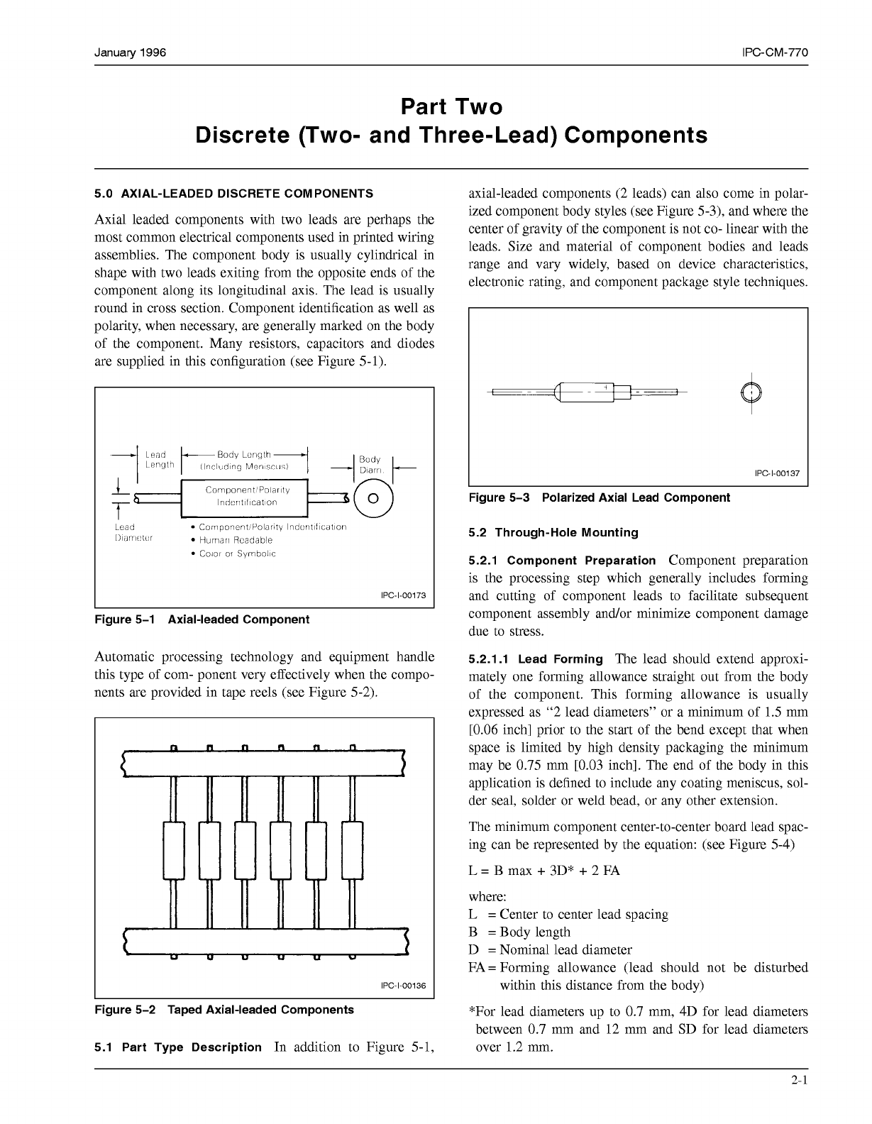
5.0 AXIAL-LEADED DISCRETE COMPONENTS
Axial leaded components with two leads are perhaps the
most common electrical components used in printed wiring
assemblies. The component body is usually cylindrical in
shape with two leads exiting from the opposite ends of the
component along its longitudinal axis. The lead is usually
round in cross section. Component identification as well as
polarity, when necessary, are generally marked on the body
of the component. Many resistors, capacitors and diodes
are supplied in this configuration (see Figure
5-1).
IPC-1-00173
I
L
Figure 5-1 Axial-leaded Component
Automatic processing technology and equipment handle
this type of com- ponent very effectively when the compo-
nents are provided in tape reels (see Figure 5-2).
I
3
\
L
U
U
U
U U
v
IPC-1-00136
I
L
Figure 5-2 Taped Axial-leaded Components
5.1 Part Type Description
In addition to Figure
5-1,
axial-leaded components (2 leads) can also come in polar-
ized component body styles (see Figure 5-3), and where the
center of gravity of the component is not CO- linear with the
leads. Size and material of component bodies and leads
range and vary widely, based on device characteristics,
electronic rating, and component package style techniques.
Figure 5-3 Polarized Axial Lead Component
5.2 Through-Hole Mounting
5.2.1 Component Preparation
Component preparation
is the processing step which generally includes forming
and cutting of component leads to facilitate subsequent
component assembly and/or minimize component damage
due to stress.
5.2.1.1 Lead Forming
The lead should extend approxi-
mately one forming allowance straight out from the body
of the component. This forming allowance is usually
expressed as “2 lead diameters” or a minimum of
1.5
mm
[0.06
inch] prior to the start of the bend except that when
space is limited by high density packaging the minimum
may be
0.75
mm [0.03 inch]. The end of the body in this
application is defined to include any coating meniscus, sol-
der seal, solder or weld bead, or any other extension.
The minimum component center-to-center board lead spac-
ing can be represented by the equation: (see Figure 5-4)
L=Bmax+3D*+2FA
where:
L
=
Center to center lead spacing
B
=
Body length
D
=
Nominal lead diameter
FA
=
Forming allowance (lead should not be disturbed
within this distance from the body)
*For lead diameters up to
0.7
mm, 4D for lead diameters
between
0.7
mm and 12 mm and SD for lead diameters
over 1.2 mm.
2-
1
COPYRIGHT Association Connecting Electronics Industries
Licensed by Information Handling Services
COPYRIGHT Association Connecting Electronics Industries
Licensed by Information Handling Services