IPC-CM-770D-1996.pdf - 第78页
IPC-CM-770 Table 16-1 Socket Types 16.1.2.2 Chip Carrier Sockets Sockets such as shown in Figure 16-9 can be used with most ceramic chip carriers. They can be surface mounted or through-hole mounted. In the surface mount…
Januaw
1996
IPC-CM-770
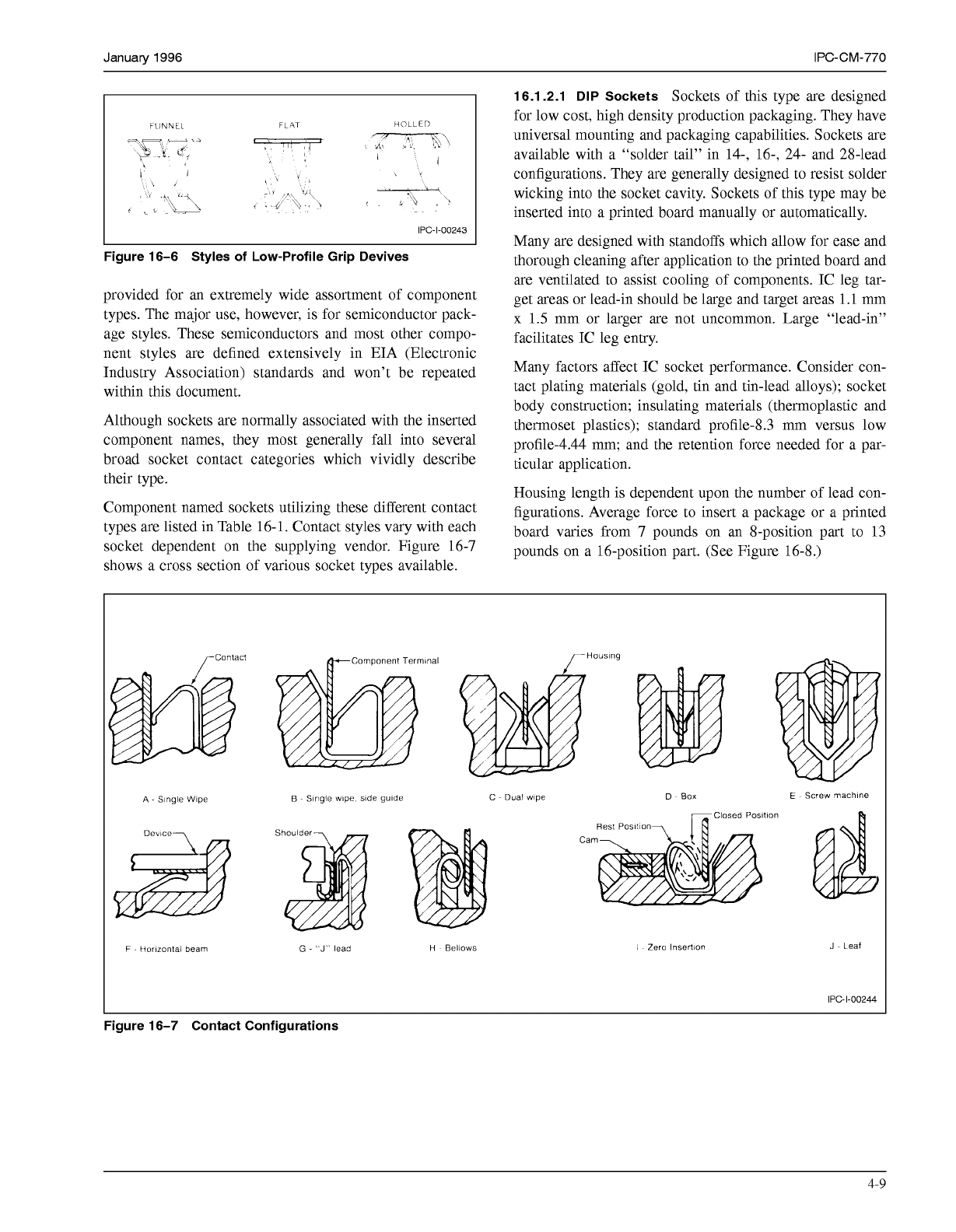
FlJNNEL
FLAT
HOLLED
IPC-1-00243
Figure 16-6 Styles of Low-Profile Grip Devives
provided for an extremely wide assortment of component
types. The major use, however, is for semiconductor pack-
age styles. These semiconductors and most other compo-
nent styles are defined extensively in EIA (Electronic
Industry Association) standards and won't be repeated
within this document.
Although sockets are normally associated with the inserted
component names, they most generally fall into several
broad socket contact categories which vividly describe
their type.
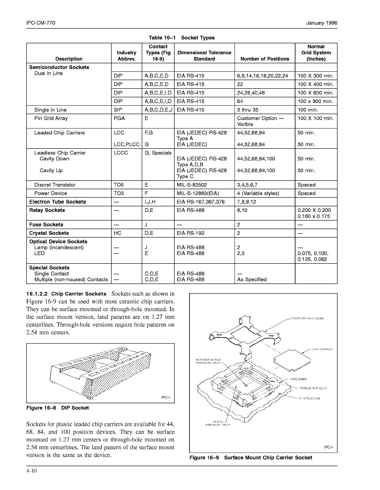
Component named sockets utilizing these different contact
types are listed in Table 16-1. Contact styles vary with each
socket dependent on the supplying vendor. Figure 16-7
shows a cross section of various socket types available.
16.1.2.1 DIP Sockets
Sockets of this type are designed
for low cost, high density production packaging. They have
universal mounting and packaging capabilities. Sockets are
available with a "solder tail" in 14-, 16-, 24- and 28-lead
configurations. They are generally designed to resist solder
wicking into the socket cavity. Sockets of this type may be
inserted into a printed board manually or automatically.
Many are designed with standoffs which allow for ease and
thorough cleaning after application to the printed board and
are ventilated to assist cooling of components. IC leg tar-
get areas or lead-in should be large and target areas
1.1
mm
x
1.5
mm or larger are not uncommon. Large "lead-in"
facilitates IC leg entry.
Many factors affect IC socket performance. Consider con-
tact plating materials (gold, tin and tin-lead alloys); socket
body construction; insulating materials (thermoplastic and
thermoset plastics); standard profile-8.3 mm versus low
profile-4.44 mm; and the retention force needed for a par-
ticular application.
Housing length is dependent upon the number of lead con-
figurations. Average force to insert a package or a printed
board varies from 7 pounds on an 8-position part to 13
pounds on a 16-position part. (See Figure 16-8.)
TContact
Houslng
A
-
Slngle Wlpe
Devlce-
B
~ Single wipe. slde gulde
C
~ Dual wlpe D ~
Box
E
~ Screw machlne
losed Posltlon
Rest
Posltlon
Cam
F
-
Horlzontal beam
G
-
"J"
lead
H
~ Bellows
1
~ Zero Insertion J ~ Leaf
IPC-1-00244
Figure 16-7 Contact Configurations
4-9
COPYRIGHT Association Connecting Electronics Industries
Licensed by Information Handling Services
COPYRIGHT Association Connecting Electronics Industries
Licensed by Information Handling Services
IPC-CM-770
Table 16-1 Socket Types
16.1.2.2 Chip Carrier Sockets
Sockets such as shown in
Figure 16-9 can be used with most ceramic chip carriers.
They can be surface mounted or through-hole mounted. In
the surface mount version, land patterns are on 1.27 mm
centerlines. Through-hole versions require hole patterns on
2.54 mm centers.
IPC-I-
I I
Figure 16-8
DIP
Socket
Sockets for plastic leaded chip carriers are available for 44,
68, 84, and
100
position devices. They can be surface
mounted on 1.27 mm centers or through-hole mounted on
2.54 mm centerlines. The land pattern of the surface mount
Januaty 1996
Normal
Grid System
(Inches)
100
X
300
min.
100
X
400
min.
100
X
600 min.
100
x
900 min.
100 min.
100
X
100 min.
50 min.
50 min.
50 min.
50 min.
Speced
Speced
7
0.200
x
0.200
0.160
x
0.175
-
0.075, 0.100,
0.125, 0.062
CHIP
CARPIER
(PRESSURE
ONLY
RETAINER SCREW
THRUSTER
CLIP
P
I
STRUCTURE
(PRESSURF
ONLY
IPC-I-
4-10
COPYRIGHT Association Connecting Electronics Industries
Licensed by Information Handling Services
COPYRIGHT Association Connecting Electronics Industries
Licensed by Information Handling Services
January
1996
IPC-CM-770
16.1.2.3 Pin Grid Array (PGA) Sockets
Sockets for
PGAs are designed to match pin configurations of the
packages. In situations where polarization is desired, a non-
active pin serves the function. Three types are available
including a standard, low insertion force and zero insertion
force. PGAs and corresponding sockets are available in
sizes from
10
x
10
to 215 x 25. At higher pin counts, zero
insertion force types are preferred. The use of high tem-
perature materials adds utility to the zero insertion force
(ZIF) style for test, conditioning, and bum-in applications.
16.1.2.4 PGA Socket
Figure 16-10 shows the various
types of pin grid array (PGA) sockets. These are available
in a wide variety of grid sizes and patterns. They are typi-
cally manufactured in an economy type (LIF) version, or a
more expensive but easier to use and durable (ZIF) produc-
tion type socket suitable for test and bum in. Note the cam
handles or levers on the ZIF designs. A typical bum in
socket is normally rated at 25000 durability cycles and
150°C
continuous operating temperature. A bum in socket
normally has a very large opening in the contact area for
ease of accepting the pin on the chip carrier.
Another type of grid device is the leadless grid array
socket. This socket, instead of mating with a pin, mates
with a pad or land on the package. This eliminates the pin
on the package but requires hold downs on the socket to
maintain normal force on the terminal.
assurance that the part is supplied as requested. The best
guarantee is a preproduction trial run of the assembly.
Preparation should focus attention on:
A. Packaging and Handling
Inadequate or improper
methods damage lead sets which will force line delays.
B.
Terminal Surface
They should be provided with tinned
or gold plate. Terminals without must be pretinned.
C. Length
of
Terminals
The terminals should not protrude
beyond the board more than
0.15
mm (nor less than
0.8
mm.
If
not provided in this fashion, they will require clip-
pin(trimming).
D.
Seals
The assembly (solder, cleaning, etc.) dictates the
degree to which the component must be closed. Standard-
precaution, however, requires use of a closed entry bottom
terminal exit or a plate to achieve the same effect. When
the socket face is to be sealed this may be accommodated
by special tapes or a pallet tool.
E.
Cleanliness
Wave solder assembly cleaning tactics are
normally adequate to assure part cleanliness. Periodic
examination, however, of preassembly components is a
normal procedure.
Sockets such as that shown in Figure 16-9 can be used in
through-hole (non-surface mounting) applications. How-
ever, since the terminals of the chip carrier are not on 2.54
Zero Insertion Force (ZIF) Socket
IPC-I-
Figure 16-1
O
Pin Grid Array Sockets
Figure 16-11 shows a leadless grid array socket with sur-
face mount leads shown in cross section. Leadless grid
array sockets are available on a 2.54 mm centerline grid
pattern (in both thru hole and surface mount versions).
16.2 Through-Hole Mounting
Sockets normally have
pre-set leads and are usually supplied by Vendor prepared
for assembly into the board. This being the situation,
preparations should be focused into two areas. Selection of
the component (and its options) for particular assembly and
mm centers, a contact similar to the one shown in Figure
16-12 is used to provide the desired transition. A polariz-
ing boss can be provided on the connector to mate with a
corresponding hole in the printed board structure.
Figure 16-12 shows a section through the short contact. A
dog-leg in the solder tail serves as a friction retaining
device. This prevents the connector from being lifted off
the mounting structure during the wave soldering opera-
tion.
4-11
COPYRIGHT Association Connecting Electronics Industries
Licensed by Information Handling Services
COPYRIGHT Association Connecting Electronics Industries
Licensed by Information Handling Services