00190802-02.pdf - 第504页
17.2 Description of Components and PCBs User’s Manual SIPLACE Line Com puter UNIX 17.2.1 PCB 1: single circuit Software V ersion 402.xx Edition 06/ 96 17 - 4 The pa ckage for m desc ription is dispens ed with . The adhe …
User’s Manual SIPLACE Line Computer UNIX 17.2 Description of Components and PCBs
Software Version 402.xx Edition 06/96 17.2.1 PCB 1: single circuit
17 - 3
PM 1 PM 3
PM 2
PCB zero point
Comp.name X Y Angle Comment
Comp1 6.60 3.84 57.00 Pos1
Comp1 10.92 0.79 10.00 Pos2
Comp1 16.26 1.30 337.00 Pos3
Comp1 20.32 4.85 276.00 Pos4
Comp1 18.29 8.92 37.00 Pos5
Comp1 13.72 10.95 22.00 Pos6
Comp1 8.64 12.98 28.00 Pos7
Comp1 5.59 17.05 94.00 Pos8
Comp1 9.40 20.60 161.00 Pos9
Comp1 14.99 21.11 190.00 Pos10
Comp1 19.05 18.32 249.00 Pos11
Comp2 28.70 0.54 270.00 Pos14
Comp2 28.70 5.62 270.00 Pos15
Comp2 28.70 10.70 270.00 Pos16
Comp2 28.70 15.78 270.00 Pos17
Comp2 30.73 20.35 180.00 Pos18
Comp2 33.27 15.78 253.00 Pos19
Comp2 34.77 10.92 253.00 Pos20
Comp2 36.24 6.06 253.00 Pos21
Comp2 38.35 1.04 270.00 Pos22
96
50
10
15
81
30
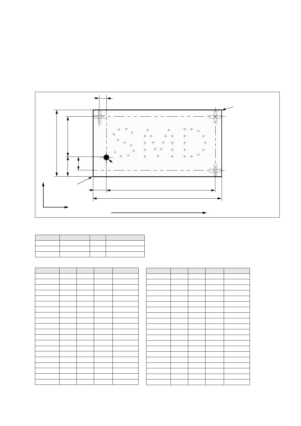
17.2 Description of Components and PCBs
17.2.1 PCB 1: single circuit
PCB 1 is a single circuit with three different components. The package forms have been taken from the stan-
dard package form library. For PCB position recognition, three fiducials are available. Fiducial 48.pm is used
which must exist in the Master data/MVS-Bibliothek (if it is not available it must be taught, see Station Computer
User´s Manual).
Comp2 40.80 6.11 288.00 Pos23
Comp2 42.37 10.95 288.00 Pos24
Comp2 43.94 15.78 288.00 Pos25
Comp2 46.48 20.35 180.00 Pos26
Comp2 49.02 15.78 270.00 Pos27
Comp2 49.02 10.70 270.00 Pos28
Comp2 49.02 5.62 270.00 Pos29
Comp2 49.02 0.54 270.00 Pos30
Comp3 58.17 0.54 180.00 Pos31
Comp3 58.17 5.62 270.00 Pos32
Comp3 58.17 10.70 270.00 Pos33
Comp3 58.17 15.78 270.00 Pos34
Comp3 58.17 20.86 180.00 Pos35
Comp3 63.25 20.86 180.00 Pos36
Comp3 68.33 19.49 210.00 Pos37
Comp3 72.04 15.78 240.00 Pos38
Comp3 73.41 10.70 270.00 Pos39
Comp3 72.04 5.62 300.00 Pos40
Comp3 68.33 1.90 330.00 Pos41
Comp3 63.25 0.54 180.00 Pos42
Comp.name X Y Angle Comment
Direction of travel
X
Y
10
5
Corner 2
PCB coordinate
system 0°
Tab. 17.2-2: Placement Positions PCB 1
Tab. 17.2-1: Component Data PCB 1
Name Package form GF-No. Handling
Comp1.be SOT23 400 Glueing, Placing
Comp2.be 1206 105 Glueing, Placing
Comp3.be 0805 103 Glueing, Placing
PCB height = 1.5 mm
Fig. 17.2.1 Dimensions of PCB 1
Corner 1
17.2 Description of Components and PCBs User’s Manual SIPLACE Line Computer UNIX
17.2.1 PCB 1: single circuit Software Version 402.xx Edition 06/96
17 - 4
The package form description is dispensed with.
The adhesive pattern description is dispensed with.
Open Component
Editor for a component
Enter component data
Component description
Adh. pattern description
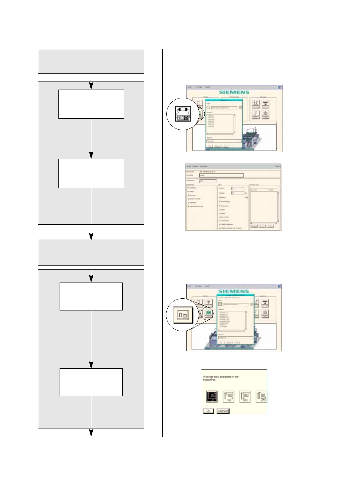
Starting PCB Editor
for a PCB
Indicate position of
PCB in the machine
PCB Description
continued on page 17-6
Package form
description
User’s Manual SIPLACE Line Computer UNIX 17.2 Description of Components and PCBs
Software Version 402.xx Edition 06/96 17.2.1 PCB 1: single circuit
17 - 5
17.2.1.1 Package Form Description
The package forms used are contained in the standard GF-library, the description is dispensed with.
17.2.1.2 Component Description
To open the Component Editor for a component, proceed as follows:
1. On the desktop click on the icon of the Component Editor .
The file selection window is opened.
2. Click on the
Selection
editing field.
3. Enter the name of the component, here:
Comp1.be
, click on the
OK
button.
The Component Editor is opened.
To enter the component data, proceed as follows:
4. Click on the
Comment
editing field.
5. Enter a comment uniquely describing the component, here:
SOT23
.
6. Click on the
Package form
editing field.
7. Enter the package form number, here:
400
.
8. Activate the appropriate button in the
Processing
selection area, here:
Placing
and
Glueing
.
9. Activate the appropriate button in the CRDL selection area, here:
No check
.
10. On the
FILE
menu click on the
Save
option.
The component data are now saved.
11. On the
FILE
menu click on the
Quit
option.
The Component Editor is closed.
12. Perform the component description for the other components, here:
Comp2.be
and
Comp3.be
.
17.2.1.3 Adhesive Pattern (DM) Description
An adhesive pattern has already been defined in the standard GF-Bibliothek for the package forms defined.
17.2.1.4 PCB Description
To open the PCB Editor for a PCB, proceed as follows:
13. On the desktop click on the icon of the PCB Editor .
The file selection window is opened.
14. Click on the
Selection
editing field.
15. Enter the name of the PCB, here:
Example_1.la
and click on the
OK
button.
A dialog box is opened.
16. Click on the
TYPE
editing field.
17. Enter a type designation, here:
SMD a
nd click on the
OK
button.
The PCB Editor is opened. The PCB is represented as a rectangle.
To specify the position of the PCB in the machine, proceed as follows:
18. Click on the Coordinate System icon.
19. Click on the PCB (rectangle).
A dialog box containing the display of four coordinate systems is opened.
20. Click on a coordinate system, here:
0°
.
21. Click on the
OK
button.
The dialog box is closed.