00190802-02.pdf - 第534页
17.2 Description of Components and PCBs User’s Manual SIPLACE Line Com puter UNIX 17.2.3 PCB 3: F ocus on Cluster T echnique Software V ersion 402.xx Edition 06/96 17 - 34 Creating a c luster continu ed on page 17-36 con…
User’s Manual SIPLACE Line Computer UNIX 17.2 Description of Components and PCBs
Software Version 402.xx Edition 06/96 17.2.3 PCB 3: Focus on Cluster Technique
17 - 33
17.2.3.1 Package form description
PCB 3 consists of four clusters with three single circuits each, all of which correspond to PCB 2.
For the package form description refer to section 17.2.2.1
17.2.3.2 Component description
PCB 3 consists of four clusters with three single circuits each, all of which correspond to PCB 2.
For the component description refer to section 17.2.2.2
17.2.3.3 Adhesive pattern description
PCB 3 consists of four clusters with three single circuits each, all of which correspond to PCB 2.
For the adhesive pattern description refer to section 17.2.2.3.
17.2.3.4 PCB description
The offset values are to be determined automatically from Fig. 17.2.7 on page 17-31 (solution on page 17-41).
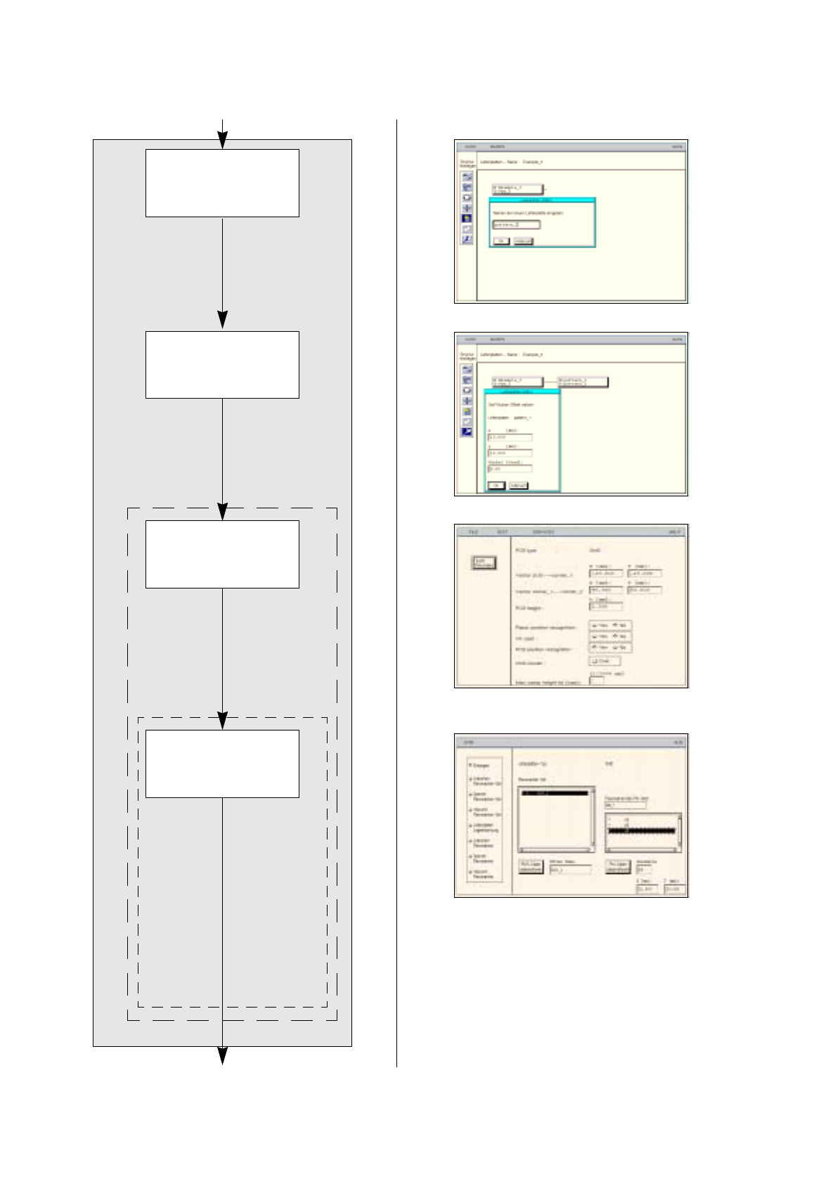
To open the PCB Editor for a PCB, proceed as follows:
1. On the desktop click on the icon the PCB Editor .
The file selection window is opened.
2. Click on the
Selection
editing field.
3. Enter the name of the PCB
,
here:
Example_3.la,
and click on the
OK
button.
A dialog box is opened.
4. Click on the
TYPE
editing field.
5. Enter a type designation, here:
Typ_1,
and click on the
OK
button:
The Component Editor is opened. The PCB is displayed as a rectangle.
To specify the position of the PCB in the machine:
6. Click on the Coordinate system icon .
7. Click on the PCB (rectangle).
A dialog box containing the display of four coordinate systems is opened.
8. Click on a coordinate system, here:
0°
.
9. Click on the
OK
button.
The dialog box is closed.
To enter the dimensions of the PCB, proceed as follows:
10. Click on the Menu icon .
11. Click on the PCB (rectangle).
12. Click on the
Cluster Editor...
option on the
SERVICES
menu.
The Cluster Editor is opened.
13. Enter the dimensions of the PCB, see Fig. 17.2.7 on page 17-31.
14. Click on the
Quit
option on the
FILE
menu.
The Cluster Editor is closed.
Defining fiducials:
no fiducials are present.
Defining ink spot:
no ink spot is present.
Entering placement positions:
the placement positions are defined at a later point in the single circuits.
17.2 Description of Components and PCBs User’s Manual SIPLACE Line Computer UNIX
17.2.3 PCB 3: Focus on Cluster Technique Software Version 402.xx Edition 06/96
17 - 34
Creating a cluster
continued on page 17-36
continued from page 17-32
Entering offset values
for the cluster
Entering dimensions
of PCB
Defining
ink spots
Cluster Editor
Fiducial Editor
PCB description
User’s Manual SIPLACE Line Computer UNIX 17.2 Description of Components and PCBs
Software Version 402.xx Edition 06/96 17.2.3 PCB 3: Focus on Cluster Technique
17 - 35
To create a cluster on the PCB, create as follows:
15. In the PCB Editor, click on the Create icon .
16. Click on the PCB, here:
Example_3
.
A dialog box is opened.
17. Click on the editing field.
18. Enter the name of the cluster, here:
pattern_1,
and click on the
OK
button.
The dialog box is closed. The new cluster is displayed at the second level.
To enter the cluster offset values, proceed as follows:
19. Click on the Coordinate system icon .
20. Click on the cluster, here:
pattern_1
.
A dialog box is opened.
21. Click on the individual editing fields and enter the offset values, see Fig. 17.2.7 on page 17-31.
22. Click on the
OK
button.
The dialog box is closed.
To enter the dimensions of the cluster, proceed as follows:
23. Click on the Menu icon .
24. Click on the cluster, here:
pattern_1
.
25. Click on the
Cluster Editor
option on the
SERVICES
menu.
The Cluster Editor is opened.
26. Enter the dimensions of the cluster, see Fig. 17.2.7 on page 17-31.
To define the fiducials for the cluster, proceed as follows:
27. In the Cluster Editor click on the
Edit fiducials
button.
The Fiducial Editor is opened.
28. Activate the
Insert
button.
29. Click on the
Fiducial set name
editing field.
30. Enter a name for the new fiducial set, here:
Set_1
.
31. Click on the
Accept fiducial set
button.
The fiducial set Set_1
appears on the fiducial list.
32. Click on the fiducial set Set_1
on the fiducial list.
33. Click on the
Fiducial
editing field.
34. Enter the fiducial number for the first fiducial, here:
48
.
35. Click on the individual editing fields for the coordinates, enter
coordinates do not confirm with the Enter key), here: see chart:
36. Click on the
Accept fiducial data
button.
The data of the fiducial are transferred to the list of the fiducials of the fiducial set.
37. Define the remaining fiducials analogously, here:
fiducials
48
and
48
.
38. Activate the
PCB position recognition
button.
39. Click on the fiducial set Set_1 on the fiducial list.
The fiducial set name Set_1
is preceded by an
L
for the PCB position recognition.
40. Click on the
Quit
option on the
FILE
menu.
The Fiducial Editor is closed.
41. Click on the
Quit
option on the
FILE
menu.
The Cluster Editor is closed.
Ficucial number X Y
48 5 5
48 5 111
48 145 5