00190802-02.pdf - 第524页
17.2 Description of Components and PCBs User’s Manual SIPLACE Line Com puter UNIX 17.2.2 PCB 2: F ocus on P ackage F or m Description Software V ersion 402.xx Edition 06/ 96 17 - 24 The adhe sive pa ttern des criptio n i…

User’s Manual SIPLACE Line Computer UNIX 17.2 Description of Components and PCBs
Software Version 402.xx Edition 06/96 17.2.2 PCB 2: Focus on Package Form Description
17 - 23
94. Activate the appropriate buttons in the Centering selection area, here:
Centering in head
.
95. In this example the default values of the editing areas Handling values, Handling instructions and Redu-
ced acceleration can be adopted, no entries are required.
To allocate a feeder to package form 1503, proceed as follows:
96. On the
SERVICES
menu click on the
Starting Feeder Editor
option.
The Feeder Editor is opened.
97. Activate the
Allocate
icon.
98. Den Button
Linie
anklicken.
The entire line is highlighted in light-green.
99. Click on the appropriate feeder on the list of placeable feeders, here:
FD~S_G_12
.
The feeder is transferred to the Feeder selection field.
100.In the Feeder Editor click on the
Save
option on the
FILE
menu.
The data are now saved.
101.Click on the
Quit
option on the
FILE
menu.
The Feeder Editor is closed.
102.In the Package Form Editor click on the
Save
option on the
FILE
menu.
The data are saved.
103.Click on the
Quit
option on the
FILE
menu.
The Package Form Editor is closed.
To enter additional information about every package form in the standard GF-Bibliothek, proceed as
follows:
104.On the desktop click on the
Data Manager
option on the
FILE
menu.
The Data Manager is opened.
105.Select the
Master data
icon by double-clicking.
The Master Data Storage is opened.
106.Select the
GF-Bibliothek
icon by double-clicking.
The package form library is opened.
107.In the command area activate the
Text
button.
The package form files are now listed as a text.
108.Click on the
Display
option on the
DISPLAY
menu, then click on the
All on
option.
A list with all additional information about every package form is displayed.
109.Click on a package form file, here:
1501.gf
.
110.On the
SERVICES
menu click on the
Additional information
option, then the
Change
option.
A dialog box is opened.
111.In the
Comment
editing field enter the comment that had been entered in the Package Form Editor.
112.In the
Author
and
Office
editing fields enter the appropriate data.
113.Click on the
OK
button.
The dialog box is closed.
114.Change the additional information for package form files
1502.gf a
nd
1503.gf,
as required.
115.In the Data Manager click on the
Quit
option on the
FILE
menu.
The Data Manager is closed.
17.2 Description of Components and PCBs User’s Manual SIPLACE Line Computer UNIX
17.2.2 PCB 2: Focus on Package Form Description Software Version 402.xx Edition 06/96
17 - 24
The adhesive pattern description is dispensed with.
Opening the
Component Editor for
a component
Entering component
data
Component Editor
Adh. pattern description
Starting the PCB
Editor for a PCB
Entering the position
of the PCB in the
machine
PCB description
continued on page 17-26
continued from page 17-22
User’s Manual SIPLACE Line Computer UNIX 17.2 Description of Components and PCBs
Software Version 402.xx Edition 06/96 17.2.2 PCB 2: Focus on Package Form Description
17 - 25
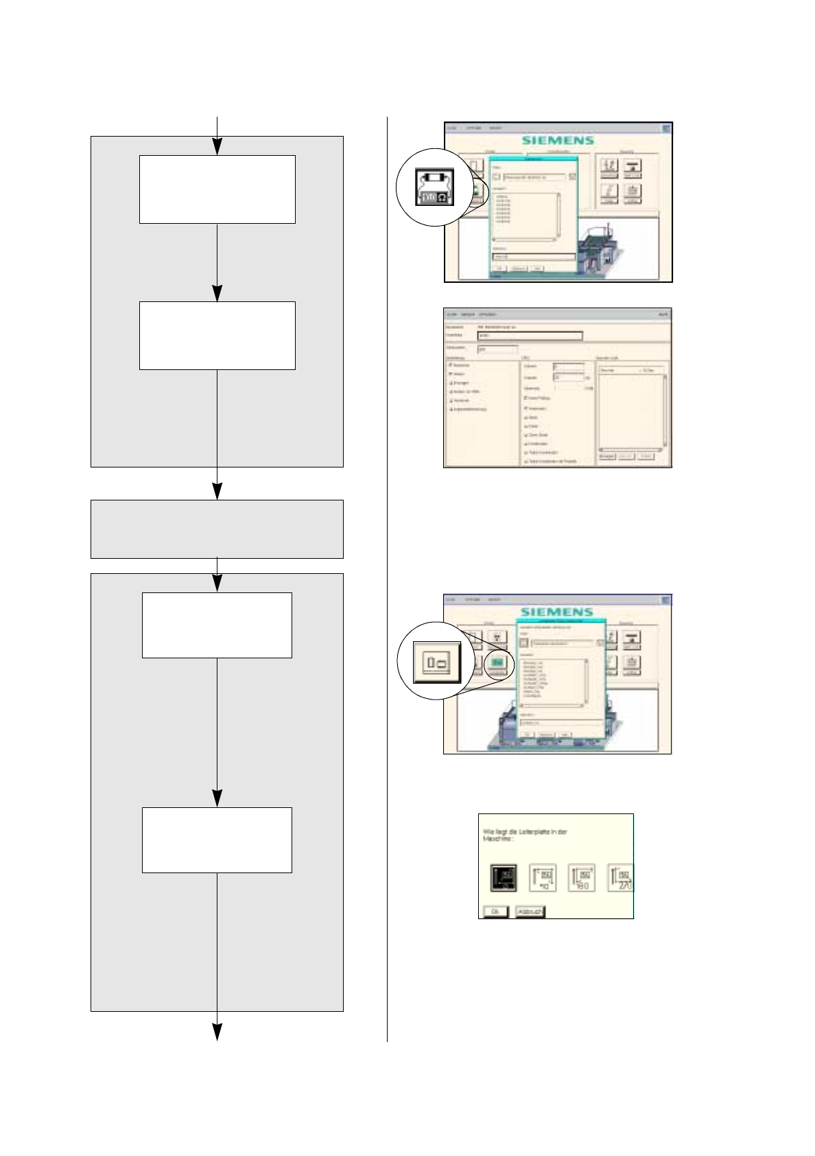
17.2.2.2 Component Description
To open the Component Editor for a component, proceed as follows:
116.On the desktop click on the icon the the Component Editor .
The file selection window is opened.
117.Click on the
Selection
editing field.
118.Enter the name of the component, here:
Comp4.be
, click on the
OK
button.
The Component Editor is opened.
To enter the component data, proceed as follows:
119.Click on the
Comment
editing field, enter a comment that is a unique description of the component, here:
Chip 2220
.
120.Click on the
Package form
editing field, enter the package form number, here:
1501
.
121.In the Handling selection field activate the appropriate buttons, here:
Placing
.
122.In the CRDL selection area activate the appropriate buttons, here:
No check
.
123.Click on the
Save
option on the
FILE
menu.
The component data are saved.
124.Click on the
Quit
option on the
FILE
menu.
The Component Editor is closed.
125.Carry out the component description for the remaining components analogously, here:
Comp5.be
and
Comp6.be
.
17.2.2.3 Adhesive Pattern Description
For the new package forms an adhesive pattern is automatically adopted from the DM-Bibliothek.
17.2.2.4 PCB Description
To open the PCB Editor, proceed as follows:
126.On the desktop click on the icon of the PCB Editor .
The file selection window is opened.
127.Click on the
Selection
editing field.
128.Enter the name of the PCB
,
here:
Example_2.la
and click on the
OK
button.
A dialog box is opened.
129.Click on the
TYPE
editing field.
130.Enter a type designation, here:
board_1
and click on the
OK
button.
The PCB Editor is opened. The PCB is displayed as a rectangle.
To specify the position of the PCB in the machine, proceed as follows:
131.Click on the Coordinate system icon .
132.Click on the PCB (rectangle).
A dialog box with the display of four coordinate systems is opened.
133.Click on a coordinate system, here:
0°
.
134.Click on the
OK
button.
The dialog box is closed.