IPC-D-859.pdf - 第14页
typically transmitted in a mode such that all the ener gy is propagated in the direction of the electric field and none in the direction of the magnetic field. Figure 3–7 illustrates the electric field and typical param- et…

3. Conductor screens
4. Overglaze screens
5. Solder screens
6. Thick film masks
7. Marking artwork or stamps
3.3.1.4 Piece-Part and Material Procurement Specifica-
tions
Piece-part and material procurement specifications
define the physical, electrical, and environmental criteria
applicable to purchased items. Special requirements should
include shipping and packaging instructions, if required.
The conventional vehicle for these documents are Specifi-
cation and Source Control drawings.
3.3.2 Viewing Unless otherwise specified, conductor lay-
ers shall be numbered consecutively, starting at the sub-
strate, as shown in Fig. 3–1.
3.3.3 Location Dimensioning All vias, test points, termi-
nal areas, and overall completed circuit dimensions shall be
dimensioned by use of a modular grid system, except
where necessary to mate parts not on grid. The choice of
the primary modular grid system used in the design of
hybrid circuits shall be metric (SI) and the basic modular
units of length shall be .5 mm and 0.05 mm; in that order
of preference, and shall be applied in the X and Y axis of
the Cartesian coordinates. The secondary modular grid sys-
tem is inch based, where the basic modular units of length
shall be 0.025 or other multiples of 0.005 inch; in that
order of preference, and shall be applied in the X and Y
axis of the Cartesian coordinates.
3.3.4 Hole Location Tolerance Unless otherwise speci-
fied, the location of holes and/or vias shall be dimensioned
with respect to single or secondary grid systems.
3.3.5 Processing Allowances The processing allow-
ances which were considered in the design and artwork
preparation for the hybrid circuit shall be documented and
defined on the master drawing in accordance with IPC-D-
325, in either note form, or by reference to another draw-
ing which contains artwork specifications (see Section 5).
3.3.6 Datums There shall be a minimum of two datum
features to establish the mutually perpendicular datum ref-
erence frame for each circuit. Each datum shall be estab-
lished by at least two holes, points, symbols, or other
datum features, but not edges, and be included on all con-
ductive layers. Critical design features may require the use
of more than one set of datum references. The master
drawing shall establish the relationship and acceptable tol-
erance between all datum features. All datum features shall
be located on grid, or establish grid criteria, as defined on
the master drawing, and should be within an outline of the
hybrid circuit.
3.4 Electrical Requirement Considerations
3.4.1 Conductor Thickness and Width
The minimum
width and thickness of conductors on the finished circuit
should be determined on the basis of the current-carrying
capacity required, and the maximum permissible conductor
temperature rise; processing allowances (see 3.3.5) shall be
considered in the evaluation. Conductor width and thick-
ness values shall be not less than the dimensions estab-
lished in Table 3–1. In general, the designer should base
dimensions on supplier data for the specific conductor
material used. For impedance/capacitance control consider-
ations see paragraph 3.4.3. For ease of manufacture and
durability in usage, these parameters should be maximized
while maintaining the minimum recommended spacing
requirements defined herein (see Table 3–1).
3.4.2 Electrical clearance Spacing between conductors
on individual layers (same plane) in multilayer hybrid cir-
cuits shall be in accordance with the requirements of Table
3–1.
3.4.3 Impedance/Capacitance Control Considerations
Multilayer hybrid circuits are ideally suited for providing
interconnection wiring that is specifically designed to pro-
vide desired levels of impedance and capacitance control.
Techniques commonly referred to as ‘‘strip-line,’’ or
‘‘embedded microstrip,’’ (see Figure 3–5) are particularly
suited for impedance and capacitance requirements.
As shown in Figure 3–5, there are four basic types of
transmission line constructions. These are:
1. Microstrip or ‘‘open-line,’’ where the external center
conductor is separated from the reference plane
(shield) by a single thickness of dielectric material.
2. Embedded microstrip, where the center conductor is
bounded on all sides by dielectric material that sepa-
rates it from a single reference plane (shield).
3. Balanced stripline, where the center conductor is
bounded on all sides by dielectric material that sepa-
rates it equally from two reference planes.
4. Unbalanced stripline, where two or more layers of con-
ductors are separated from a combination of reference
planes in an unbalanced configuration.
The characteristic impedance of a microstrip can be calcu-
lated using the formula:
Z
0
=
87
√
e
r
+ 1.41
ln
(5.98h)
(0.8W + t)
where e
r
= relative dielectric constant of substrate material
(see Table 3–5)
w,h,t are dimensions indicated in Figure 3–7.
The most commonly used microwave circuit technique is
microwave stripline (Figure 3–6A). Stripline energy is
December 1989 IPC-D-859
7
typically transmitted in a mode such that all the energy is
propagated in the direction of the electric field and none in
the direction of the magnetic field.
Figure 3–7 illustrates the electric field and typical param-
eters involved in microstrip design.
When the conductor is covered with a dielectric material
such as solder mask (embedded microstrip), the impedance
characteristics will be reduced depending on the thickness
and dielectric constant of the material (approximately 5
percent).
IPC-859-3-1
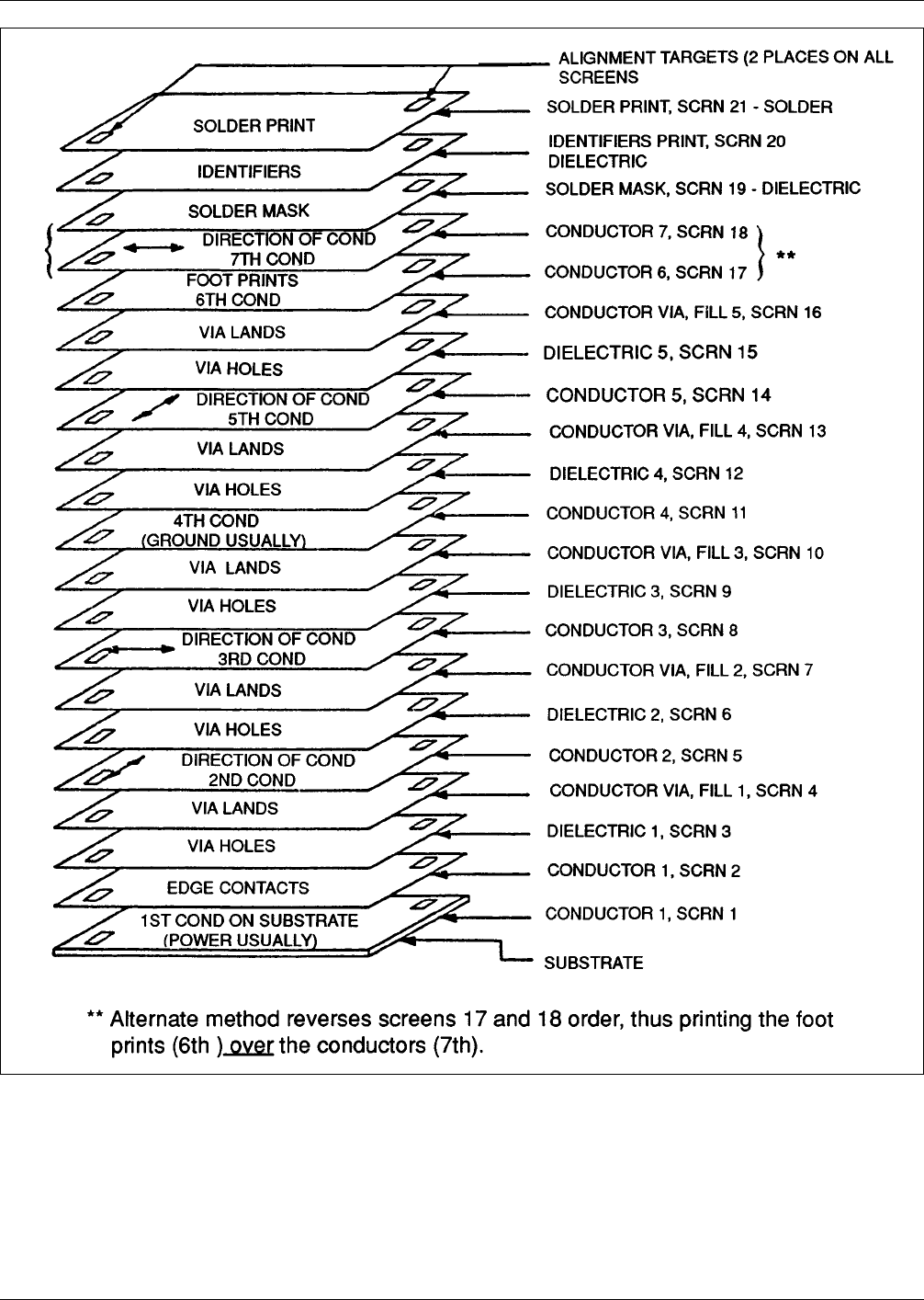
Figure 3–1 Screening masks typically required for thick film processing
IPC-D-859 December 1989
8

Plane sequences should be arranged so that the signal lay-
ers are symmetrical about the ground or voltage plane. This
may be accomplished several ways provided that any adja-
cent signal layers, not separated by a ground or voltage
plane must have their key axes running perpendicular to
each other. (see Figure 3–1).
DC power and ground planes also function as AC reference
planes. Power and ground connector pins should be evenly
distributed along the edge of the board for AC reference.
3.4.3.1 Capacitance Considerations The capacitance
associated with a single crossover (see Figure 3–8) is very
small and is typically a fraction of a picofarad. As the
number of crossovers per unit length increases, the intrin-
sic capacitance of the transmission line also increases. The
crossover lumped capacitance adds to the intrinsic line
capacitance. Crossover capacitance may be approximated:
C(pF)=5.72 E
r
(l + 0.8h)
(W + 0.8h)
h
provided that l ≥ 0.5h
W ≥ 0.5h
Where:
E
r
= dielectric constant
h = dielectric thickness between crossovers
(mm)
l = length (mm)
W = width (mm)
The distributed coupling capacitance between two parallel
conductors on the same layer (see Figure 3–9), assuming
0.015 mm [0.0006 inch] print thickness, is given by
C
C
=
N
∑ 6.7x10
–4
l
n
d
n
pF
n = 1
Where: l
n
= length of parallelism between the conduc-
tors
for separation d
n
d
n
= perpendicular distance between
the conductors
The above equation is a first order approximation which
disregards capacitance contributed by all other conductors
distributed across the entire substrate. It is assumed that the
first order contributions constitute 90% or more of the cou-
pling capacitance, and that coupling between adjacent con-
ductors is the prime concern.
Circuit design shall specify the allowable capacitances
from which the required spacing and maximum parallelism
shall be determined.
Table 3–1 Dimensional Constraints for Thick-Film Conductors and Lands
Conductor and Land Sizes and Spacing
Minimum
Dimension
mm [inch]
Nominal
Dimension
mm [inch]
Maximum
Dimension
mm [inch] Figure Item
Conductor to edge of substrate for conductors
≤0.38 mm [0.015 inch]
0.25 [0.010] 0.51 [0.020] None 3–2
1
Conductor to edge of substrate for conductors
>0.38 mm [0.015 inch]
0.25 [0.010] 0.32 [0.0125] None 3–2
2
Exit bonding lands (width and length) 0.25 [0.010] 0.32 [0.0125] None 3–2
3
Wire bonding lands (width and length—one or two
wires on same land) (preferred)
0.25 [0.010] 0.32 [0.0125] None 3–2
4
Wire bonding lands (width and length—one wire per
land (special)
0.25 [0.010] 0.32 [0.0125] None 3–3
5
Conductor width (preferred) 0.25 [0.010] 0.51 [0.020] None 3–2
6
Conductor width (special) 0.13 [0.005] 0.25 [0.010] None 3–3
7
Conductor-to-conductor spacing (preferred) 0.25 [0.010] 0.51 [0.020] None 3–2
8
Conductor-to-conductor spacing (special) 0.13 [0.005] 0.25 [0.010] None 3–3
9
Conductor-to-resistor spacing (on untrimmed
side of resistor)
0.25 [0.010] 0.38 [0.015] None 3–4
10
Conductor-to-resistor spacing (on trimmed side of
resistor)
0.38 [0.015] 0.51 [0.020] None 3–4
11
Conductor-to-resistor spacing, top-hat configuration 0.76 [0.030] 0.89 [0.035] None 3–2
15
Upper and lower conductor widths at crossover junc-
tion
0.25 [0.010] 0.38 [0.015] None 3–4
12
Crossover conductor-to-connecting-conductor
overlap-length
0.25 [0.010] 0.32 [0.0125] None 3–4
13
Conductor crossover dielectric overlap 0.25 [0.010] 0.38 [0.015] None 3–4
14
Dielectric to resistor spacing 0.51 [0.020] 0.51 [0.020] None 3–4
16
December 1989 IPC-D-859
9