IPC-D-859.pdf - 第18页
The shortest possible conductor length should be used between devices. The hybrid circuit should be separated into areas for high, medium, and low frequency circuits. 3.4.5 Circuit Type Considerations 3.4.5.1 Digital Cir…
one capacitor for not more than five logic devices and
one for no more than two memory devices.
4. Minimize the impedance and radiation loop of the
decoupling capacitor by keeping capacitor leads as
short as possible, and locating them adjacent to the
integrated circuit.
The power and ground planes are solid when using the
gold system.
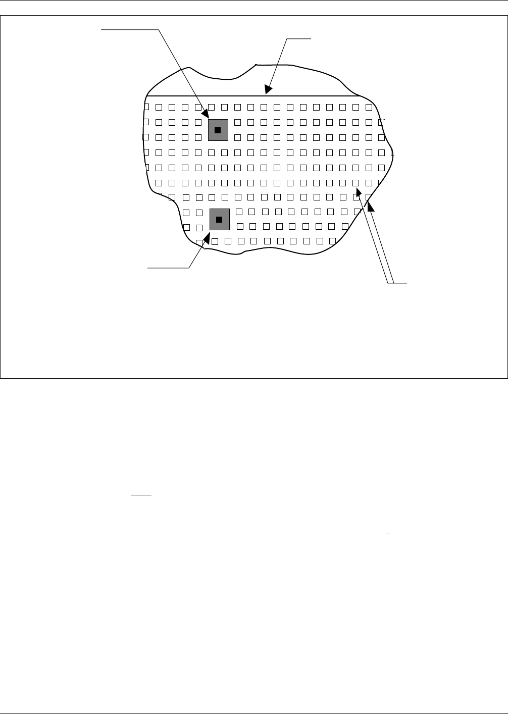
The power and ground planes are typically gridded with
0.4 mm [0.015 inch] conductors, and 0.25 mm [0.010 inch]
spaces as shown in Figure 3–10 when using the copper
system.
In digital power distribution schemes, the grounding and
power should be designed first, not last, as is typically
done. All interfacing, including power, should be routed to
a single reference edge, or area. Avoid opposing end inter-
connections. At the interconnection reference edge, all
ground structures are to be made as heavy as possible.
IPC-859-3-3
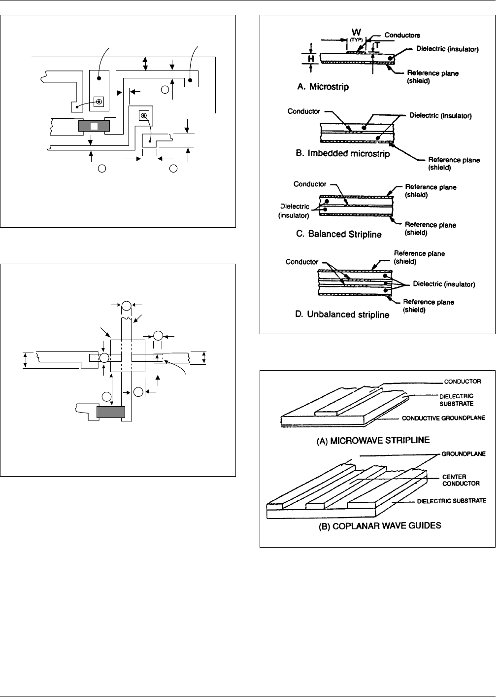
Figure 3–3 Special fineline conductor dimensions
(nominal) and positioning constraints (see Table 3–1)
EDGE OF
SUBSTRATE
NOTE: A conductor adjacent to the edge of the substrate must be a minimum
of 0.25 mm [0.010 inch] wide and at least 0.25 mm [0.010inch] in from the edge.
0.32 [0.0125]
0.25 [0.010] min. (see note)
0.25 [0.010] min.
(see note)
0.25
[0.010]
0.25
[0.010]
0.32
[0.0125]
R
9
5
7
IPC-859-3-4
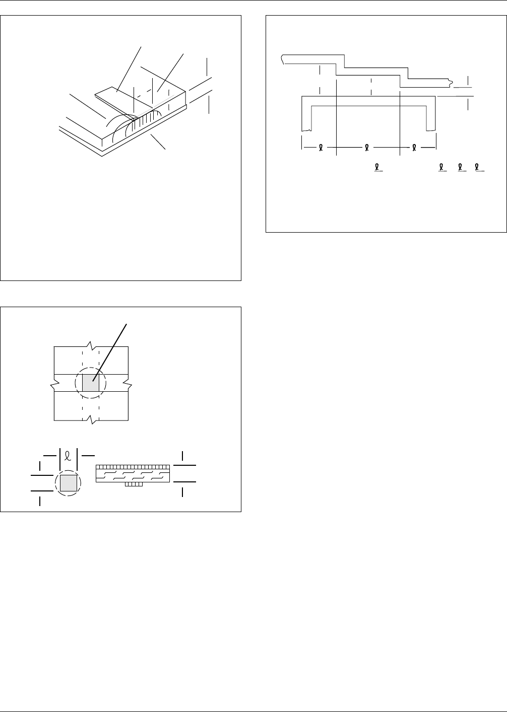
Figure 3–4 Nominal thick film crossover dimensions
(see Table 3–1)
12
13
12
16
14
0.38
[0.015]
0.38
[0.015]
0.38
[0.015]
0.32
[0.025]
0.76 [0.030]
0.38 [0.015]
CROSSOVER
DIELECTRIC
LOWER LEVEL
CONDUCTOR
UPPER LEVEL
CONDUCTOR
SEE NOTE
NOTE:
This conductor
dimension should
be at least 0.13 mm
[0.005 inch] wider
than the width of
the upper conductor.
SEE
NOTE
IPC-859-3-5
Figure 3–5 Transmission line multilayer hybrid circuit
construction
IPC-859-3-6
Figure 3–6 Typical microwave circuit types
December 1989 IPC-D-859
11
The shortest possible conductor length should be used
between devices. The hybrid circuit should be separated
into areas for high, medium, and low frequency circuits.
3.4.5 Circuit Type Considerations
3.4.5.1 Digital Circuits
Digital circuits are composed of
electronic components that can provide state information (1
or 0), as a function of the performance of the overall cir-
cuit. Normally, logic integrated circuits are used to perform
this function; however, discrete components may also be
used sometimes to provide digital responses.
Integrated circuit devices use a variety of logic families.
Each family has its own parameters regarding the speed of
the digital transmission, as well as the temperature rise
characteristics necessary to provide the performance. In
general, a single board usually uses the same logic family
in order to facilitate a single set of design rules for conduc-
tor length for signal driving restrictions. Some of the more
common logic families are:
• TTL—Transistor Transistor Logic
• MOS—Metal Oxide Semiconductor Logic
• CMOS—Complimentary Metal Oxide Semiconductor
Logic
• ECL—Emitter Coupled Logic
• The following guidelines should be used on all logic
designs to improve the testability of the multilayer
printed board assembly.
1. Connect the set, clear, or reset of all flip-flops to reset
terms. Power up reset is ideal. See Figure 3–11.
2. Connect the clear or master reset of counters to reset
terms or provide preset logic. See Figure 3–12.
3. Provide a method to disable free-running oscillators,
and provide a pin-out to an unused I/O on the oscilla-
tor clock line.
4. Provide outputs to unused I/O pins for feedback or
‘‘deep’’ logic loops. This also applies for serial logic.
5. Keep direct output control, wherever possible, on all
LSI devices to enhance their testability.
6. Provide jumper lines from the delay line clock circuits
to unused I/O pins, so that intermediate clocks may be
controlled.
IPC-859-3-7
Figure 3–7 Stripline electric field
▼
▼
▼
▼
▼
TYPICAL PARAMETERS
h = 0.635mm [0.025"]
w = 0.061mm [0.0024"]
t = 0.00635mm [0.00025"]
Er = 10 (Al O )
Z = 50
EEFF = 6.8
▼
Electric
Field Lines
Conducting
Ground Plane
Dielectric
Substrate
Conducting
Strip
23
Ω
h
▼
t
▼
▼
W
▼
IPC-859-3-8
Figure 3–8 Crossover capacitance
Shaded Area
Indicates Crossover
▼
▼
▼
▼
▼
A
A
▼
▼
IPC-859-3-9
Figure 3–9 Example of parallel line coupling capacitance
calculation
▼
▼
▼
▼
▼
▼
▼
▼
σ
1
σ
2
σ
3
1 3
▼
▼
▼
▼
C Total = 6.7 x 10 = 6.7 x 10
c
}
n
n
σ
1
σ
1
2
σ
2
3
σ
3
++
pF)(
n=1
3
3
{
Σ
-4 -4
IPC-D-859 December 1989
12
7. Provide test points to appropriate conductors in untest-
able circuits.
8. The maximum unterminated line length for a high
speed digital circuit is given by:
l
mw
=
t
r
2t pd
where:
t
r
= rise time (10–90%) in nanoseconds
t pd = propagation delay (see Table 3–2)
9. Provide wrap-a-round test capability of resistors.
10. Provide test points to control lines in memory circuits
for off-line testing.
3.4.5.2 Analog Circuits Analog circuits are usually
made from discrete devices, and provide the wave-form
characteristics necessary to describe a circuit. Standard dis-
crete components (resistors, capacitors, diodes, transistors,
etc.), as well as power transformers, coils and chokes, are
usually the types of components used for analog circuits.
Some of the rules to be followed when designing analog
printed board assemblies are:
1. Always determine correct polarity of the component, if
applicable.
2. Transistor emitter/base and collector should be prop-
erly identified (ground transistor case where appli-
cable).
3. The maximum allowable lead length for analog signal
interconnections shall be in the order of:
l
MAX
=
λ
8
mm [inch]
where: λ = signal wave length in mm [inches]
In instances where line lengths approach maximum, an
evaluation shall be made to insure that excessive
impedance mismatches that may result will not
adversely affect electrical performance.
4. If different grounds are used, keep grounding busses as
far away as possible.
5. As opposed to digital signals, analog design should
have signal traces considered first, as ground planes, or
ground conductors can be used to complete circuit con-
nections.
IPC-859-3-10
Figure 3–10 Power and ground planes along with conductor areas exceeding 6.45 square mm [0.01 square inch] (0.38
mm [0.015 inch] conductors and 0.25 mm [0.010 inch] spacing on a 0.64 mm [0.025 inch] grid [CAD]).
POWER OR
GROUND PLANE
PAD
SPACES
VIA
0.25 MM X 0.25 MM
[0.010 INCH X 0.010 INCH]
0.38 MM [0.015 INCH] X
0.38 MM [0.015 INCH]
0.89 MM [0.035 INCH]
SQUARE PAD COVERING
4 SPACES
PROVIDES A 1.65 MM
[0.065 INCH]
SQUARE SOLID AREA
NOTE:
For via contact to copper gridded power or ground plane, via should terminate
on a square solid conductor area of 1.,65 mm x 1.65 mm [0.065 inch x 0.065 inch].
December 1989 IPC-D-859
13