IPC-D-859.pdf - 第52页
5.3.2.1 Bond Lands W ire bond land sizes shall be in accordance with Figure 5–13. Figure 5–14 shows recommended locating dimensions to provide access and clearance for the bonding tool head. 5.3.2.2 Component Mounting La…
E. The maximum number of conductor levels for high
yields is three. Processing yields may be affected with
additional layers, although an infinite number of layers
are theoretically possible.
F. Semiconductor chips, capacitor chips, and resistor
chips may be mounted on lands on the top conductor
level of multilayer thick-film designs. Also, ultrasonic
wire bonds may be made from the chips to the lands;
however, it is recommended that thermo-compression
bonds be made only to bottom level conductors. If
thermo-compression bonds must be made to the top
conductor level, a double conductor layer should be
used for the land (see Figure 5–12)
G. Provide test points for short-circuit and continuity
checking between conductor levels.
5.3.2 General Requirements for Lands and Bond Lands
The following general requirements shall be met for all
lands and bond lands.
IPC-859-5-6
Dim
Producibility mm
[inch]
Most ↔ Least
ABC
Resistor
distance to dielectric
H 1.27
[0.050]
1.14
[0.045]
1.14
[0.045]
Conductor lines staggered,
1
distance to dielectric step
(typical on 2-layer circuit).
H
1
0.51
[0.020]
0.38
[0.015]
0.25
[0.010]
Conductor lines overlap
L
1
0.38x
0.38
[0.015]
0.25x
0.25
[0.010]
0.25x
0.25
[0.010]
Dielectric crossover,
distance extended beyond
width (on either top or
bottom conductor).
H
1
0.51
[0.020]
0.38
[0.015]
0.38
[0.015]
1. A staggered dielectric configuration is required whenever two (closely
placed) adjacent conductors are screened over a dielectric crossover.
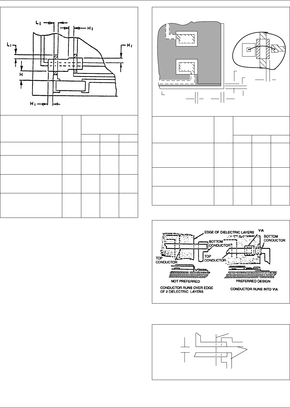
Figure 5–6 Minimum dielectric distance from other lines
and for crossovers.
IPC-859-5-7
Dim
Producibility mm
[inch]
Most ↔ Least
ABC
Dielectric distance to
metallized land for solder
or epoxy component
attachment.
W 0.38
[0.015]
0.25
[0.010]
0.25
[0.010]
Dielectric distance to edge
of substrate, minimum
sized
W
1
0.25
[0.010]
0.13
[0.005]
0.13
[0.005]
Dielectric width, when
covering conductors that
run under bond wire.
W
2
0.25
[0.010]
0.13
[0.005]
0.13
[0.005]
Figure 5–7 Minimum dielectric spacing and size
▼
▼
▼
▼
▼
▼
▼
▼
▼
Substrate
Edge
W
2
W
1
W
1
W
W
2
Solder
Pad
Solder
Pad
▼
▼
DEVICE
IPC-859-5-8
Figure 5–8 Conductor interconnects external to the
dielectric
IPC-859-5-9
Figure 5–9 Spacing between adjacent conductors
running over a dielectric edge.
▼
0.38mm
[0.015"] min.
Dielectric Edge
Bottom
Conductors
▼
▼
▼
▼
December 1989 IPC-D-859
45
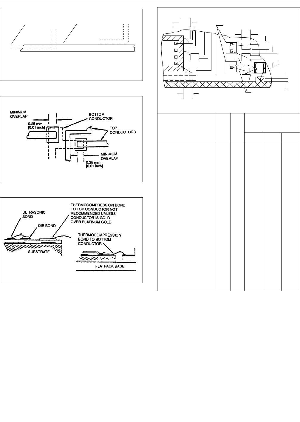
5.3.2.1 Bond Lands Wire bond land sizes shall be in
accordance with Figure 5–13.
Figure 5–14 shows recommended locating dimensions to
provide access and clearance for the bonding tool head.
5.3.2.2 Component Mounting Lands Figure 5–15 estab-
lishes minimum lands for component mounting.
Nominal dimensions and spacing for chip mounting lands
are shown in Table 5–1 and Figure 5–16.
5.3.2.3 Exit Land/Package Lead Alignment Layouts
should be prepared with the exit bonding lands on the sub-
strate in alignment with the metallized bonding areas or
pins of the hybrid package. An example of proper and
improper location of lands is shown in Figure 5–17.
Figure 5–18 illustrates a recommended approach for iden-
tifying exit lead/pins for standard packages.
5.3.2.4 Probe Lands When space allows, probe lands
should be included for trouble-shooting and for use with
resistor trimming. For this latter purpose, lands should be
placed as close as possible to resistor terminations as
shown in Figure 5–19. (Note: The recommended size for
probe lands is 0.51 mm [0.020 inch] square.)
5.3.2.5 Lands ‘‘MELF’’ Discrete Components MELF
discrete components, when mounted as defined in 4.3.3,
shall have their land relationships identified as shown on
Figure 5–20.
IPC-859-5-10
Figure 5–10 Preferred parallel conductor design
Top
Conductor
▼
Bottom
Conductor
▼
One conductor directly over
another
Conductors not over or under
each other
Poor Design Preferred Design
IPC-859-5-11
Figure 5–11 Overlap between top and bottom conductors
IPC-859-5-12
Figure 5–12 Examples of die bonds and wire bonds in
multilayer thick-film designs
IIPC-859-5-13
Dim
Min/
Max
Producibility mm
[inch]
Most ↔ Least
ABC
Wire Bond Land Sizes:
• Length
L Min 0.51
[0.020]
0.38
[0.015]
0.30
[0.012]
• Width, single wire
W Min 0.38
[0.015]
0.25
[0.010]
0.20
[0.008]
• Width, double wire
W
2
Min 0.64
[0.025]
0.51
[0.020]
0.38
[0.015]
Locating angle, die edge to
center of wire bond site.
< Min 90° 45° 45°
Die edge distance to edge
of land:
• Maximum
D
1
Max 1.78
[0.070]
2.54
[0.100]
2.54
[0.100]
• Minimum or 2.5 x thick-
ness of die (whichever
is greater).
D
2
Min 1.27
[0.050]
0.76
[0.030]
0.64
[0.025]
Dielectric distance to center
of wire bond site
D
3
Min 0.5
[0.020]
0.38
[0.015]
0.25
[0.010]
Wrap around metallization
distance to center of wire
bond site.
T Min 0.76
[0.030]
0.64
[0.025]
0.64
[0.025]
Figure 5–13 Wire bond land sizes and locations (wire
bonds shall not be placed on via fill metallization.)
▼
▼
▼
▼
▼
YES
NO
IC
DEVICE
DEVICE
W
W
L
2
D
1
D
2
D
3
T
▼
▼
▼
▼
▼
▼
▼
▼
▼
▼
▼
▼
▼
▼
▼
90°
45°
90°
IPC-D-859 December 1989
46
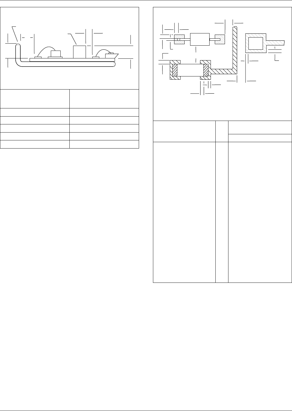
5.3.2.6 Land Pattern for Leadless Chip Carriers The
attachment lands for surface mounting leadless chip carri-
ers should be the same width as the component terminal
(castiliation maximum) plus 0.13 mm [0.005 inch] when-
ever possible. The land length should extend between 0.4
to 1.0 mm [0.016 inch to 0.04 inch] beyond the maximum
chip carrier outline on all foursides to create a horizontal
solder fillet length equal to the vertical fillet rise (see Fig-
ure 5–21). The design of fan-out to interconnect the basic
land pattern to other circuitry/devices is dependent on wir-
ing density, testability, assembly, repairability, and routabil-
ity requirements. Figure 5–22 shows some examples of
possible fan-out patterns for leadless chip carriers. Chip
carrier land sites should be located on a fixed grid within
the hybrid circuit to optimize testing. This grid should be
compatible with assembly and testing equipment, so as to
minimize the amount of specialized and complex equip-
ment necessary.
5.3.2.7 Lands for Leaded Chip Carriers The land size
for ceramic and for leaded chip carriers should match the
lead configurations. J shaped leads should have the land
width be equal to or 0.12 mm [0.005 inch] larger than the
width of the lead. The length should extend between 0.4 to
1.0 mm [0.016 inch to 0.040 inch] beyond both sides of the
foot of the J pattern. Other types of leads used for chip
carriers should have the land commensurate with the lead
configuration, in order to create a horizontal solder fillet
length at the toe and heel of the lead configuration, as
shown on Figure 5–23.
5.3.2.8 Lands for Ribbon Leaded Surface Mounted
Parts
The land requirements for mounting ribbon leaded
parts, such as ‘‘flat packs’’, ‘‘quad packs’’, or small outline
devices, shall preferably be rectangular. The minimum land
width shall be equal to or exceed the maximum lead width,
providing room for both solder fillets at both the heel and
toe of the ribbon lead. The minimum land width shall be
approximately one and one-half times the width of the lead,
or 0.12 mm [0.005 inch], whichever is less (see Figure
5–24). Flat pack termination shall be staggered to permit
greater spacing wherever possible. The center position of
ribbon leaded components should be on a fixed grid, wher-
ever possible, to facilitate testing.
5.3.2.9 Lands for Flattened Round Leads Flattened
IPC-859-5-14
Obstacle Height
H mm [inch]
Wire Bond-to-Obstacle
Minimum Spacing
W mm [inch]
0.25 [0.020] 1.02 [0.040]
1.02 [0.040] 1.14 [0.045]
1.52 [0.060] 1.27 [0.050]
2.03 [0.080] 1.40 [0.055]
Over 2.54 [0.100] 1.15 [0.065]
Figure 5–14 Locating wire bond lands and sizing
components so as to provide access/clearance for
bonding tool head.
Obstacle
Obstacle
W
W
H
H
▼
▼
▼
▼ ▼
▼
▼
▼
▼
▼
IPC-859-5-15
Dim
Producibility mm [inch]
Most ↔ Least
ABC
Discrete leaded component:
• Metallized land overlap,
for epoxy or solder
attachment.
A 0.38
[0.015]
0.25
[0.010]
0.25
[0.010]
• Distance from leaded
component
F 1.02
[0.040]
1.02
[0.040]
1.02
[0.040]
Semiconductor chip:
• Die bond land overlap,
for eutectic or epoxy
attachment.
B 0.38
[0.015]
0.25
[0.010]
0.25
[0.010]
• Land distance from
other metallization
E 0.51
[0.020]
0.38
[0.015]
0.38
[0.015]
Leadless component (chip
capacitor or chip resistor):
• Ceramic body overlap
onto land
C 0.38
[0.015]
0.25
[0.010]
0.25
[0.010]
• Metallized end land
overlap onto land, for
epoxy or solder
D 0.51
[0.020]
0.38
[0.015]
0.38
[0.015]
• Distance from leaded
component
F 1.02
[0.040]
1.02
[0.040]
1.02
[0.040]
Figure 5–15 Minimum lands for component mounting
Leadless
Component
(Chip Capacitor
or Resistor)
▼
Semicon-
ductor
Chip
Discrete
Leaded
Component
▼
▼
▼
▼
▼
▼
▼
▼
▼
▼
▼
▼
▼
▼
▼
▼
▼
▼
▼
▼
▼
E
B
B
E
F
D
C
C
A
A
A
December 1989 IPC-D-859
47