IPC-D-859.pdf - 第55页
round leads shall have a land which will provide the seat- ing so that the heel and the terminal relationship is in accordance with Figure 5–25. Leads shall be seated with no side overhang. T oe overhang is acceptable, p…
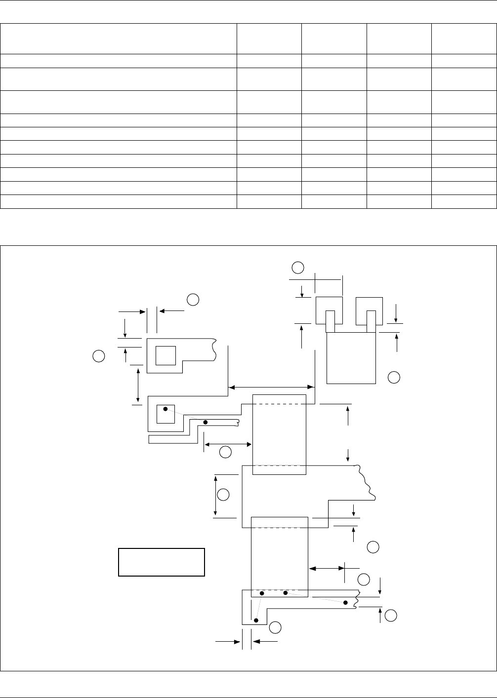
Table 5–1 Chip Mounting Lands
Land Size and Spacing
Minimum
Dimension
mm [inch]
Nominal
Dimension
mm [inch]
Maximum
Dimension
mm [inch]
Figure 5–16
Item
Semiconductor chip-to-chip spacing (1) (1) None
1
Semiconductor chip mounting land (width and length
beyond chip)
0.25 [0.010] 0.32 [0.0125] None
2
Passive chip-to-bonding land wiring distance beyond chip
(width or length)
0.76 [0.030] 0.82 [0.0325] 0.100
3
Passive chip mounting land (beyond chip width) 0.13 [0.005] 0.19 [0.0075] None
4
Passive chip mounting land (beyond chip end) 0.38 [0.015] 0.43 [0.017] None
5
Passive chip-to-conductor overlap 0.25 [0.010] 0.32 [0.0125] None
6
Passive chip-to-wire bonding land spacing 1.02 [0.040] 1.27 [0.050] None
7
Inductor lead mounting land (width and length) 1.02 [0.040] 1.27 [0.050] None
8
Inductor body-to-wire bonding land 0.13 [0.005] 0.19 [0.0075] None
10
Passive chip end-to-end spacing 1.02 [0.040] 1.21 [0.050] None
9
(1) Use 0.81 [0.032 inch] spacing between chips.
IPC-859-5-16
Figure 5–16 Nominal dimensions for chip mounting lands (see Table 5–1)
R
C
L
CR
CR
9
6
3
5
4
7
10
1
2
8
1.27 [0.050]
1.52 [0.060]
0.32 [0.0125]
0.32 [0.0125]
0.8 [0.032]
Minimum
1.27 [0.050]
This distance
dependent on
chip width
This distance
dependent on
chip width
0.19
[0.0075]
1.27 [0.050]
0.32 [0.0125]
0.19 [0.0075]
0.44 [0.0175]
Dimensions
in mm 0.82 [0.0325]
IPC-D-859 December 1989
48
round leads shall have a land which will provide the seat-
ing so that the heel and the terminal relationship is in
accordance with Figure 5–25. Leads shall be seated with no
side overhang. Toe overhang is acceptable, provided that
the flattened lead in contact with the terminal area is a
minimum of 150% of the unflattened lead diameter, and the
overhang does not reduce the spacing to adjacent parts to
less than that specified on the assembly drawing.
5.3.2.10 Lead Frame Bonding Lands Figure 5–26 estab-
lished minimum values for size and location of lead frame
bonding lands.
5.3.3 Wire Bonds Wire-bond connection should never be
made between lands on IC chips. A method for making
such connections is illustrated in Figure 5–27
Wires should never cross other wires or chip components.
When wire bonds cross electrically uncommon conductor
IPC-859-5-17
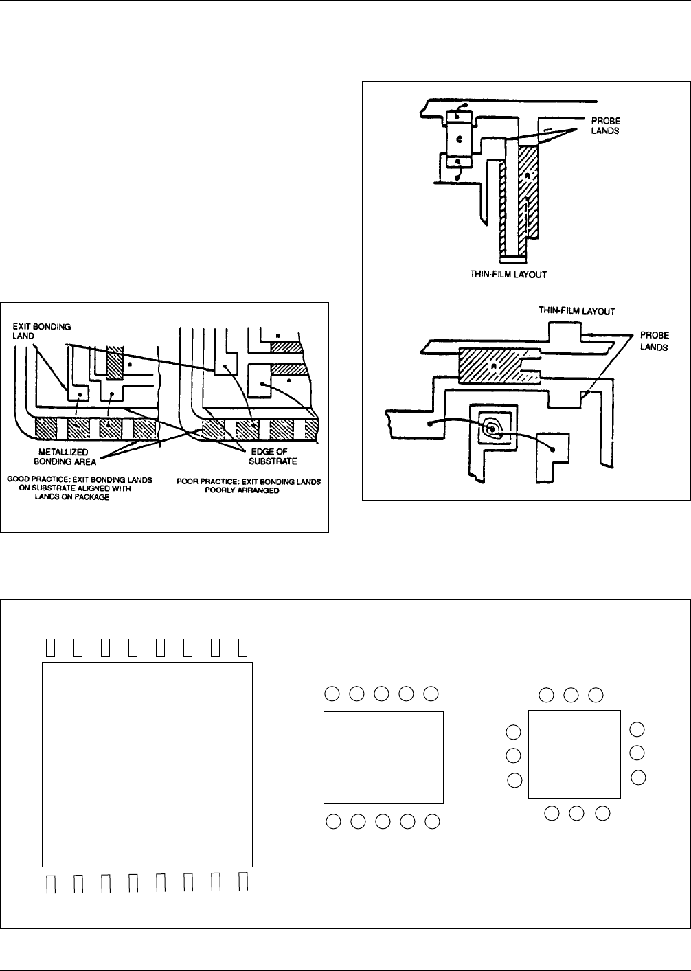
Figure 5–17 Exit land/alignment/misalignment
considerations for hybrid packages
IPC-859-5-18
Figure 5–18 Examples of lead/pin identification assignments
19 X 19 [0.75" X 0.75"] SUBSTRATE
OUTLINE FOR 16 LEAD
25 X 25 [1" X !"] HAC PAC
PACKAGE
8.76 X 11.2 [0.345 X 0.445]
SUBSTRATE
OUTLINE FOR
10 PIN
12.7 X 12.7 [0.5 X 0.5]
PLATFORM
PACKAGE
8.4 X 8.4 [0.33 X 0.33]
SUBSTRATE
OUTLINE FOR
15.24 [0.0600]
DIA. TO 20.32 [0.800]
PACKAGE
16 15 14 13 12 11 10 9
1 2 3 4 5 6 7 8
10 9 8 7 6 9 8 7
1 2 3 4 5
10
11
12
6
5
4
1 2 3
DIMENSIONS IN mm [INCHES]
IPC-859-5-19
Figure 5–19 Probe land positioning to assist resistor
trimming.
December 1989 IPC-D-859
49
IPC-859-5-21
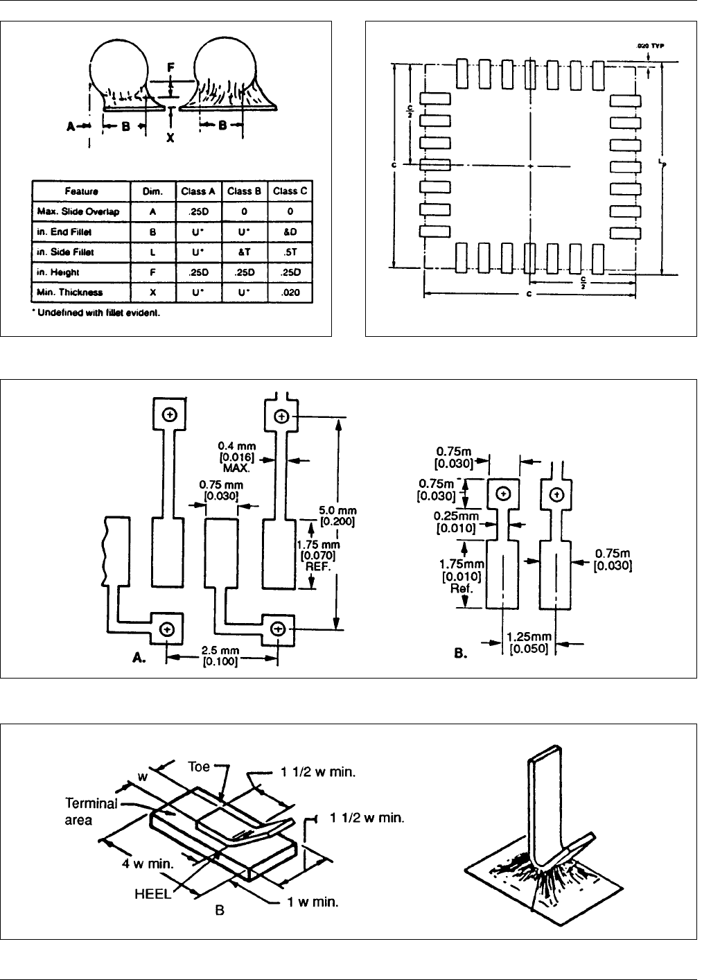
Figure 5–21 Land pattern leadless chip carrier
IPC-859-5-20
Figure 5–20 MELF chip resistors land relationships
IPC-859-5-22
Figure 5–22 Fan-out patterns
IPC-859-5-23
Figure 5–23 Land to heel/toe configurations
IPC-D-859 December 1989
50