IPC-D-859.pdf - 第40页
IPC-859-4-4 Figure 4–4 SO 16 integrated circuit package IPC-859-4-5 Figure 4–5 SOT -89 package drawing example IPC-D-859 December 1989 34
for optimized testing. This grid should be compatible with
assembly and testing equipment, so as to minimize the
amount of specialized and complex equipment.
For designs where fan-out patterns are not on 0.100 inch
grids (see Figure 4–10, a specialized fixture would be
required for electrical testing.
4.3.1.5 Primary-Side Testing Testing on the primary
side is only recommended for unpopulated P/I structures.
Thus, designing a chip carrier site for primary side testing
does not required dedicated through vias, and thus permits
more efficient routing. This is usually only used with
designs using blind or buried vias, or where the secondary
side is inaccessible. Testing on a 2.54 mm [0.100 inch] grid
is suitable on an ‘‘IL’’ modified fan-out pattern. (See Fig-
ure 4–11)
Testing on an ‘‘II’’ pattern (Figure 4–11) is possible, but
would require dedicated test fixtures with customized 1.27
mm [0.050 inch] pitch probes.
4.3.1.6 Secondary-Side Testing Testing on the second-
ary side is suitable for both populated and unpopulated P/I
structures. In both cases, it should be recognized that nets
ending on non-via lands on the primary side of the P/I
structure will require a via for continuity testing. Thus,
testing on the secondary side requires an ‘‘IL’’ or modified
fan-out patterns with vias and test lands on 2.54 mm [0.100
inch] grid on the secondary side, and corresponding rout-
ing penalty. An ‘‘II’’ land pattern and its associated vias,
not on a 2.54 mm [0.100 inch] grid, would again require a
dedicated test fixture as described for primary side testing.
4.3.2 Leadless Discrete Components (Figure 4–12)
Microminiature leadless devices are available to the circuit
designer in resistor, capacitor, transistor, and zener diode,
chip form. The chips are placed in a nonconductive carrier
and encapsulated in epoxy, or hermetically sealed. All met-
allized surfaces are plated to permit thermo-compression or
ultrasonic bonding.
4.3.2.1 End-Capped Discrete Components End-capped
discrete resistor and capacitor components, and similar
leadless end-capped discrete components, shall not be
stacked, nor shall they bridge spacing between other parts
or components, such as terminals or other properly-
mounted components (see Figure 4–13.)
End-cap discrete leadless components with electrical ele-
ments deposited on an external surface, such as chip resis-
tors, shall be mounted with that surface facing away from
the printed board (see Figure 4–14).
4.3.3 MELF Component metal electrical face leadless
devices are also available in circular fashion. These cylin-
drical devices have the land-to-lead configuration require-
ments shown in Figure 4–15. The same rules for proper
mounting, as discussed in section 4.3.2, apply.
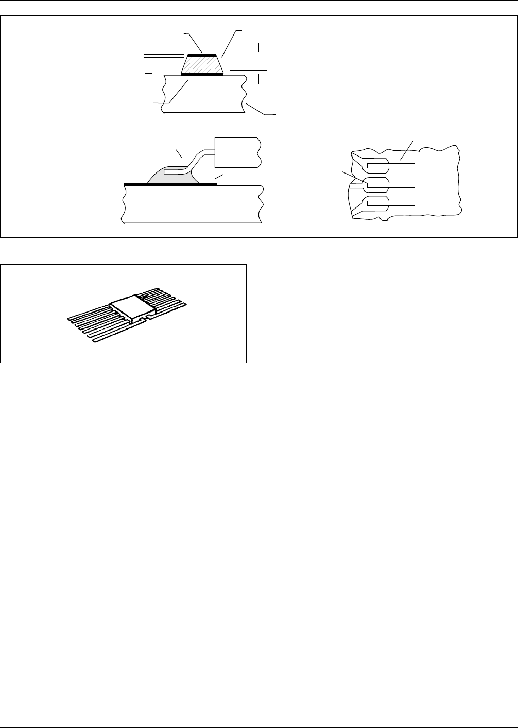
IPC-859-4-2
Figure 4–2 Flat-pack surface mounting
▼
Tinned Lead
▼
▼
Reflowed
Solder
Flat Pack Lead
▼
▼
Land
Flat Pack Lead
Land
Solder
Laminate
3T Maximum
Lead Thickness (T)
▼
▼
▼
▼
▼
▼
▼
IPC-859-4-3
Figure 4–3 Flat-pack multiple-lead component
December 1989 IPC-D-859
33
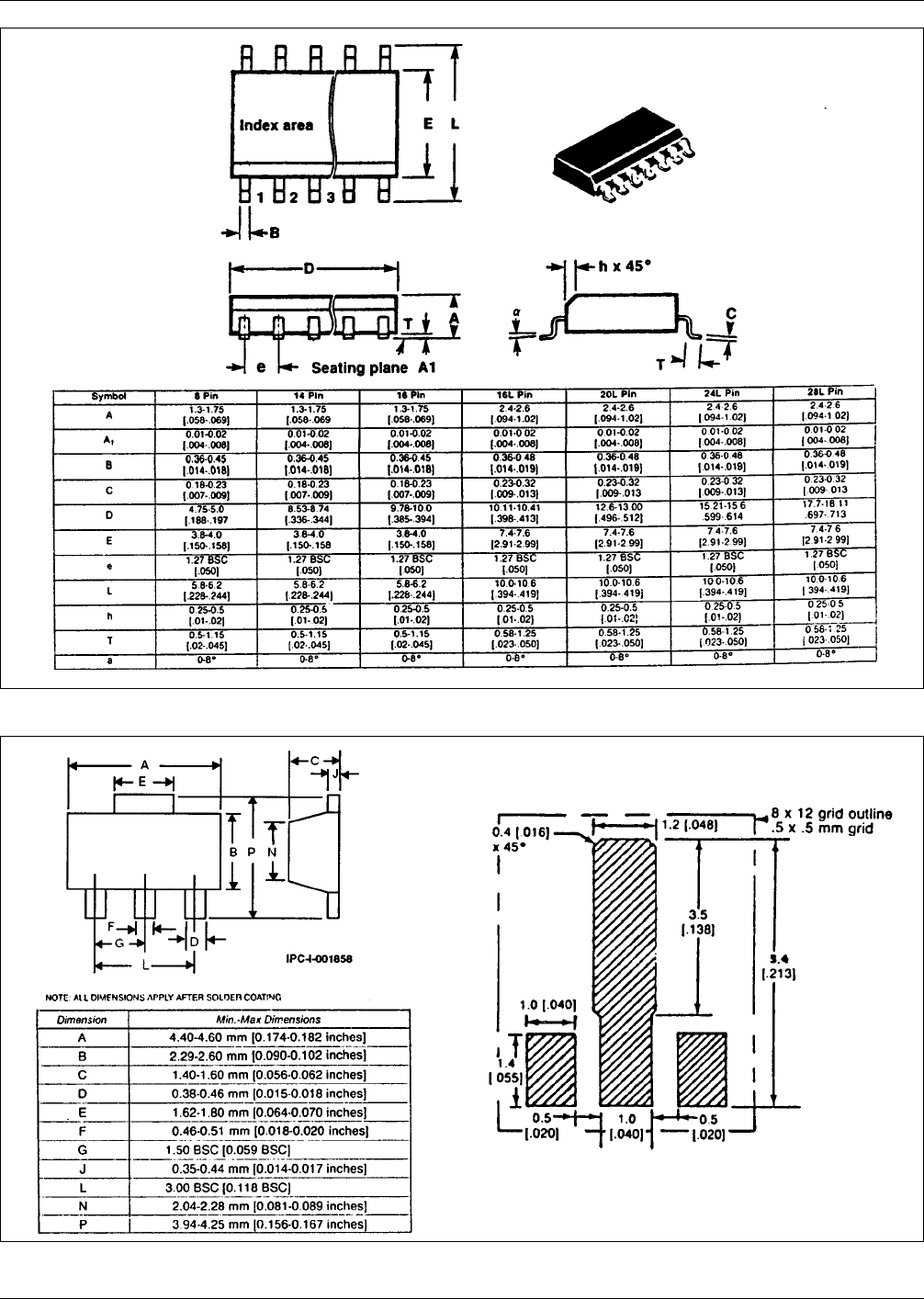
IPC-859-4-4
Figure 4–4 SO 16 integrated circuit package
IPC-859-4-5
Figure 4–5 SOT-89 package drawing example
IPC-D-859 December 1989
34
4.4 Component Lead Sockets
4.4.1 Integrated Circuit Sockets
4.4.1.1 DIP Sockets
Sockets, such as that shown in Fig-
ure 4–16 are designed for low-cost, high-density, mounting
of DIP components. They are generally designed to resist
solder wicking into the socket or cavity, and have provi-
sions that provide the needed clearance of the socket above
the substrate.
4.4.1.2 Chip Carrier Socket Sockets such as that shown
in Figure 4–17 can be used with most of the chip carriers
described in 4.3.1. They can be either surface mounted or
through-hole mounted, depending on the termination con-
figuration of the socket contacts.
When they are surface mounted, they can also be obtained
with a mechanical contact pressure interface to the printed
board. The advantages of this type of socket are the ease of
replacement of the socket, and the absence of damage due
to soldering and unsoldering. A disadvantage is that a sec-
ond mechanical interface is now in the circuit path.
4.5 Connectors and Interconnects One of the critical
design requirements for multilayer hybrid circuits is to pro-
vide a method of interconnection for signal and power
input/outputs.
This is normally done by surface contact to lands on the
outer layer(s), typically with a conductive header or by the
use of flexible circuitry.
When the header is used, it may be soldered, welded or
brazed to the surface lands, with its contacts projecting
beyond the periphery of the substrate. In selecting material
for the header, consideration should be given to such items
IPC-859-4-6
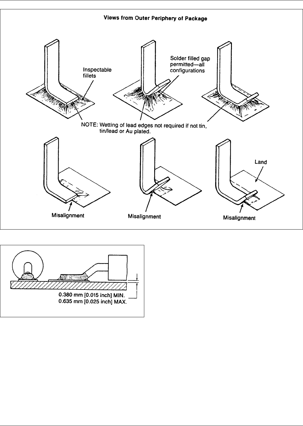
Figure 4–6 Plastic-leaded chip carrier lead misalignment
IPC-859-4-7
Figure 4–7 Round or coined lead
December 1989 IPC-D-859
35