IPC-D-859.pdf - 第21页
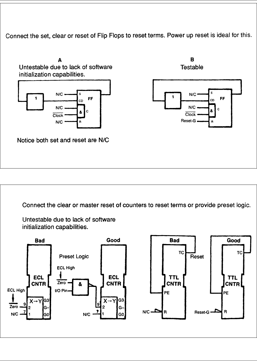
IPC-859-3-11 Figure 3–1 1 Flip-flop testability IPC-859-3-12 Figure 3–12 Master clear for counters December 1989 IPC-D-859 15
6. Keep heat sensitive and heat radiating components as
far apart as possible (incorporate heat sinks whenever
necessary).
3.4.5.3 Conductor Spacing In high frequency analog
and high speed digital circuits, a minimum of one line
width shall be maintained as spacing between any two
adjacent signal conductors. Very critical signals shall have
line width and spaces or shielding as required to insure
sufficient isolation and to minimize noise coupling as
specified.
3.5 Thermal Requirement Considerations Hybrid elec-
tronic technology is capable of performing within the tem-
perature range of –55° to +125°C. In fact, the basic thick-
film technology can perform satisfactorily at temperatures
significantly beyond this range. The limiting factor is most
often the performance of the attached active components or
the inherent power dissipation of the circuit.
Power dissipation has a major influence on circuit parti-
tioning and ultimate package size. Also, all material and
component operating capabilities are limited by inherent
maximum operating temperatures, above which their per-
formance may either degrade seriously or catastrophic fail-
ure may occur. With semiconductors, this temperature is
usually specified in terms of a maximum junction tempera-
ture. For other components, the maximum body tempera-
tures and hot-spot temperatures are commonly used as the
figures of merit.
In any case, the maximum operating temperature of an
electronic material or component is a direct result of the
electrical power dissipated in the element and/or the tem-
perature and heat-transfer characteristics of the environ-
ment associated with the component. All components,
especially resistors and active devices, will dissipate heat
in the performance of their normal electrical function.
Therefore, the problem is to remove the heat as quickly as
possible to prevent temperature rises within the heat-
generating elements.
Because of their small size and high component densities,
microcircuits are subject to high power densities and poor
heat transfer capabilities. As a result, thermal power den-
sity, rather than component density, may be the limiting
factor in certain microcircuit designs.
Thermal design considerations and thermal analysis tech-
niques are very important steps in the design cycle. There-
fore, the hybrid designer should have a thorough knowl-
edge of thermal design guidelines, the thermal properties of
materials, thermal analysis techniques and the thermal
evaluation of thick-film circuits.
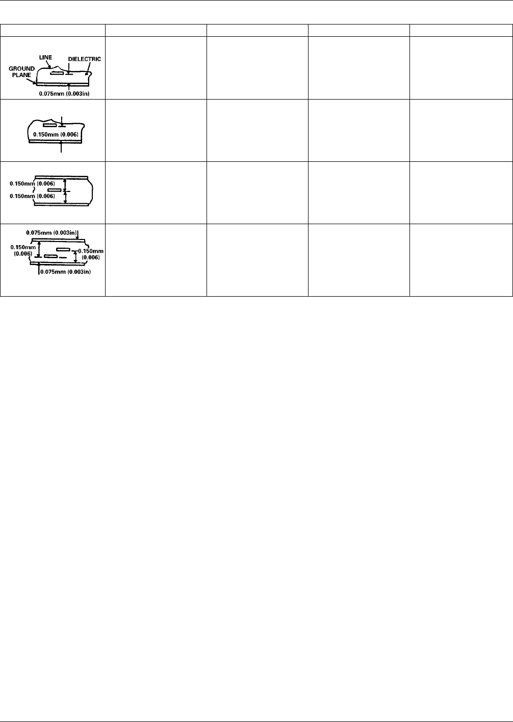
Table 3–2 Conductor Electrical Parameters (10 Mil wide Conductors, Experimental Results)
Configuration Parameter Units* Gold System** Copper System***
Microstrip
z0.152 mm [0.006]
Dielectric
Thickness (h)
C
R
tpd
Z
0
S
21
E
R
0.311
0.015
0.0079
33.30
–7.20
5.70
0.220
0.014
0.0079
43.40
–5.87
3.30
Microstrip
z0.152 mm [0.006]
Dielectric
Thickness (h)
C
R
tpd
Z
0
S
21
E
R
0.185
0.015
0.0079
46.20
–5.93
5.20
0.141
0.015
0.0075
62.30
–5.31
2.90
Stripline
z0.305 mm [0.012]
Dielectric
Thickness (h)
t ≅ 0.0127 mm
[0.0005]
C
R
tpd
Z
0
S
21
E
R
0.295
0.015
0.0087
35.50
–5.91
5.30
0.202
0.0122
0.0079
46.10
–4.94
2.80
Unsymmetrical
Stripline
z0.2286 mm [0.009]
Dielectric
Thickness (h)
t ≅ 0.0127 mm
[0.0005]
C
R
tpd
Z
0
S
21
E
R
0.370
0.0106
0.0087
30.00
–6.47
4.80
0.276
0.0106
0.0083
36.20
–5.31
2.50
*C (Capacitance) pF/mm; R (Resistance) Ohm/mm; t pd (Propagation Delay) ns/mm;
Z
0
(Characteristic Impedance) Ohms; S
21
(Forward Transmission Loss at 300 MHz) dB;
E
R
(Apparent Dielectric Constant—estimated from Z
0
)
**Solid ground and voltage planes used for Gold System
***Gridded ground and voltage planes (0.38 mm lines and spaces) used for Copper System
IPC-D-859 December 1989
14
IPC-859-3-11
Figure 3–11 Flip-flop testability
IPC-859-3-12
Figure 3–12 Master clear for counters
December 1989 IPC-D-859
15

The following are important heat transfer considerations.
3.5.1 Material Selection Select materials with good
thermal conductivity. Table 3–3 is a useful guide for mate-
rial selection.
3.5.2 Substrate Dimensions Use a thick substrate for
best heat transfer and distribution unless it is to be bonded
to a heat sink, in which case the thinnest possible substrate
should be used.
The substrate area required for a given electronic circuit is
greatly dependent upon power levels of components. Thus,
low power level circuitry can be packaged more densely
than power circuits.
The use of some first approximation ‘‘rules-of-thumb’’ for
the number of devices (chips) that can be accommodated
with a given technology in various package sizes, would
provide a starting point, together with the thermal consid-
erations, for deciding if the given circuitry needs to be par-
titioned. Another deciding factor in partitioning is the
input/output (I/O) requirements of the circuitry.
3.5.3 General Guidelines
A. Distribute power sources as evenly as possible over the
substrate surface to reduce hot spots and to maintain a
uniform thermal profile.
B. Locate the highest-power sources over or near heat
sinks.
C. Do not locate high-power sources near substrate cor-
ners or edges unless heat sinking is provided in that
vicinity.
D. Design power resistors as large as possible and assure
that sufficient area will be maintained after adjustment.
E. High-heat dissipating components should be attached to
the substrate in such a manner as to provide the lowest
possible thermal resistance between the components
and the substrate.
F. Components should not be attached over the other heat
dissipating elements, i.e., chip capacitors over thick-
film resistors.
G. For best thermal performance, make the junction
between a backside-mounted semiconductor chip and
the substrate with a material of low thermal resistance
that is as thin as possible, and provide a uniform con-
tact area that is free from voids. (In this regard a
knowledge of process capability is critical. If the worst-
case die-attachment wettability is 50%, base heat trans-
fer calculations on the reduced area.)
H. When wire leads or pins are attached to a substrate:
(1) make leads or pins as short as possible, (2) select a
pin material of high thermal conductivity and a pin size
with the maximum possible cross-sectional area,
(3) use as many leads as possible, and (4) locate heat
sources as near to the pins as possible.
I. In final packaging: (1) select a package configuration
that will provide the best thermal conductivity for a
specific application, (2) provide a good thermal con-
duction path between the substrate and the package
case, and (3) avoid air spaces in the thermal conductiv-
ity path if possible. Plastics with high thermal conduc-
tivity can be used to fill voids and improve heat trans-
fer.
3.5.4 Heat Dissipation Calculations The rise in tem-
perature of each component can be estimated using a
model of thermal resistance and power dissipation in which
the temperature rise is calculated as:
T=RxP
where T = temperature rise of the device
above the hybrid case (°C)
R = total thermal resistance between the
device
and the hybrid case (°C/W)
P = power dissipated in the device (W)
The total thermal resistance is calculated by summing the
thermal resistances of each material in the thermal path
between the device and hybrid case (see Figure 3–13).
Thus:
R
t
=R
1
+R
2
+R
3
+R
4
+R
5
where R
T
= total thermal resistance from the top of the
device to the bottom of the hybrid case.
If parallel thermal paths are involved, the parallel thermal
resistances are totaled in the same manner as are parallel
electrical resistances.
The thermal resistance of a particular material layer is cal-
culated as:
R =
t
KA
Table 3–3 Typical Hybrid Materials Thermal Conductivity
Material
Thermal Conductivity
W/°C/mm
Silicon 58.4
Kovar 9.1
Molybdenum Tab 99.1
Alumina (Al
2
O
3
) 17.5
Beryllia (BeO) 139.7
Conductive Epoxy 1.02
Epoxy Preform 0.25
AuSi Eutectic Bond 144.8
AuSn Solder 114.3
IPC-D-859 December 1989
16