IPC-D-859.pdf - 第63页
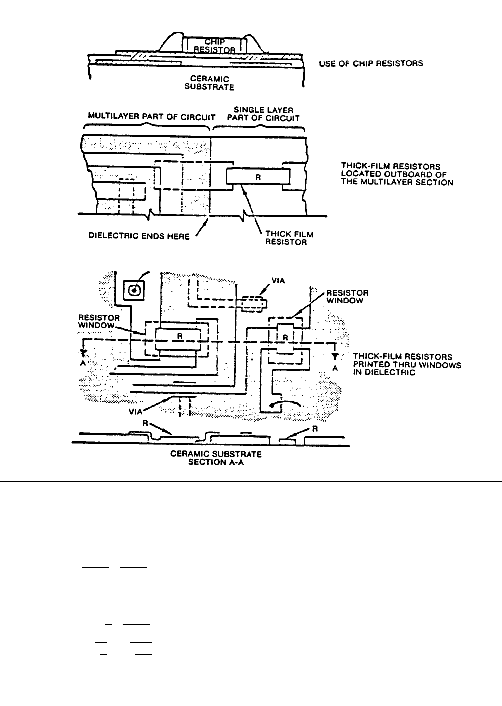
5.3.4.3.5 Screening Resistors may be screened directly onto the substrate or on any equi-planar level. They must never be designed into a dielectric ‘ ‘hole’ ’ or terminated by dif ferent layers of conductors. Resistors …
For example, suppose one must design a 39 Kohm resistor
using 10 Kohm/square paste. It must dissipate 500 mW.
(1) A =
P
0.0775
=
0.500
0.0775
= 6.45 mm
2
A =
P
50
=
0.500
50
= 0.01 m
2
(2) N =
R
ρ
=
39,000
10,000
= 3.9
(3) W =
√
A
N
=
√
6.45
3.9
= 1.29 mm
=
√
[0.01]
3.9
=[0.051 inch]
(4) L = NW = 3.9 x 1.29 = 5.05mm
= 3.9 x [0.051]=[0.199 inch]
The resistor example would have to be dimensioned for
digitizing, would be screened at the exact value (hopefully
not higher) and would run at maximum dissipation. This is
not good design practice. If the design permits, one could
arbitrarily boost the area from 6.45 mm
2
[0.01 inch
2
]to
9.68 mm
2
[0.015 inch
2
] so that the resistor would run
cooler. Then one could recalculate the width and round it
off to the nearest grid or split grid. Finally, it is necessary
to recalculate the length and round it down to the next
lower grid or split grid.
IPC-859-5-33
Figure 5–33 Three methods showing the use of resistors with multilayer thick-film designs (see Figure 5–34 for window
allowance).
IPC-D-859 December 1989
56
5.3.4.3.5 Screening Resistors may be screened directly
onto the substrate or on any equi-planar level. They must
never be designed into a dielectric ‘‘hole’’ or terminated by
different layers of conductors. Resistors should not be
screened on screened dielectric directly over underlying
conductors.
5.3.4.3.6 Piggy Back/Daughter Substrates If space or
paste limitations make it necessary, resistors may be
screened onto a small piggy-back or daughter board sub-
strate. The small substrate is then bonded to the main sub-
strate. Connections between the two substrates are made
with wire, ribbon, or solder bonds.
5.3.4.3.7 Probe Lands Probe lands must be available for
measurements during trimming. Probe ‘‘shadow’’ must
always be a consideration. Normally the run to the resistor
terminal is adequate but if this run is covered by dielectric
than a separate land at least 0.38 x 0.38 mm [0.015 x 0.015
inch] must be available.
5.3.4.3.8 Overglaze All resistors screened with 10, 30 or
100 ohm/square paste must be protected with overglaze as
must all conductors leading to them.
5.3.5 Vias Design techniques and precautions to be used
in designing multilayer vias include:
Table 5–4 Dimensional Constraints for Thick-Film Resistors
Resistor Sizes and Spacing
Minimum
Dimension
mm [inch]
Nominal
Dimension
mm [inch]
Maximum
Dimension
mm [inch]
Figure
Item
Resistor height (H), top hat configuration 0.76 [0.030] None 12.7 [0.500] 5–32
Resistor width (W), top hat configuration 1.52 [0.060] 2.03 [0.080] None 5–32
Resistor-to-resistor spacing 0.38 [0.015] 0.51 [0.020] None 5–35
1
Resistor-to-conductor overlap (length) 0.25 [0.010] 0.32 [0.0125] None 5–35
3
Resistor-to-conductor overlap (width) 0.13 [0.005] 0.19 [0.0075] N (1) 5–35
4
Resistor length (ink value ≤100 K ohms/sq) 0.76 [0.030] 1.02 [0.040] N (1) 5–35
4
Resistor length (ink value >100 K ohms/sq) 1.02 [0.040] 1.52 [0.060] N (1) 5–35
3
Resistor width (ink value ≤100 K ohms/sq) 0.76 [0.030] 1.02 [0.040] N (1) 5–35
6
Resistor width (ink value ≤100 K ohms/sq) 1.02 [0.040] 1.52 [0.060] N (1) 5–35
7
Conductor land length (beyond resistor) 0.13 [0.005] 0.25 [0.010] None 5–35
8
Air abrasive trimming allowance (from resistor
to adjacent conductor, resistor, or land)
1.27 [0.050] 0.51 [0.020] None 5–36
9
Air abrasive trimming allowance for top-hat designs 0.76 [0.030] 0.89 [0.035] None 5–36
10
Resistor overglaze overlap (2) 0.13 [0.005] 0.19 [0.0075] None 5–36
11
(1) N=Aspect ratio=L/W 0.2≤Nfor rectangular designs of resistors whose tolerance is <20 percent. N=30 maximum for top-hat
resistor designs after trimming
(2) Overglaze is required for resistors made from inks of a sheet resistivity of less than 32 ohms per square.
IPC-859-5-34
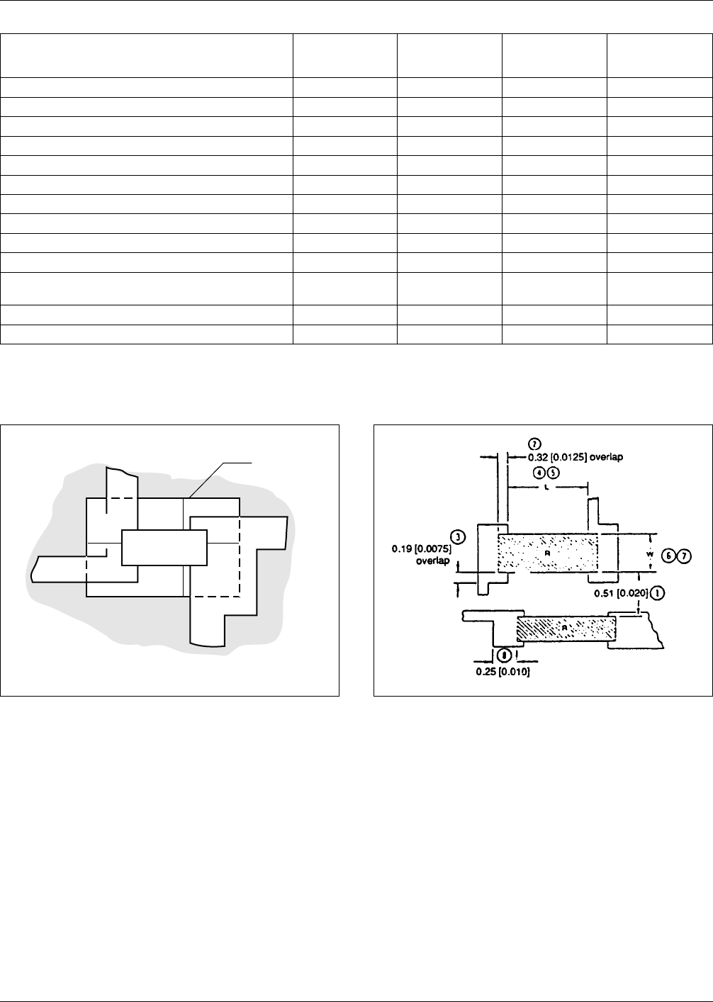
Figure 5–34 Window allowance for thick-film resistors.
Window for
Resistor
▼
R
▼
▼
▼
▼
▼
▼
0.75
[0.030]
0.75
[0.030]
▼
▼
0.75
[0.030]
0.75
[0.030]
0.75
[0.030]
IPC-859-5-35
Figure 5–35 Nominal thick-film rectangular resistor
dimensions (see Table 5–5)
December 1989 IPC-D-859
57
A. Via window sizes and spacings should be as shown in
Figure 5–41.
B. The selection of a via design will depend on the spe-
cific layout of the adjacent conductor levels; Figure
5–42 illustrates typical examples. Allow as much over-
lap between the top and bottom conductors as possible
within the design constraints.
C. The vias should be staggered as shown in Figure 5–43,
when routing a conductor from an upper level to the
bottom level. Although this uses more room than does
the routing of a conductor directly through a single
window, yield and reliability are improved. (The print-
ing of a conductor through the thickness of two dielec-
tric layers can result in low yields.)
D. If design or space restrictions prevent the staggering of
vias on adjacent levels, an alternate means of routing a
conductor through multiple levels should be used such
as that is shown in Figure 5–44. With this arrangement
a blind through-hole land is printed through the via
window on the second level to contact the bottom con-
ductor. The top (or third level) conductor is then printed
through another via window to contact the blind land
on the second level.
5.4 Coatings and Markings
5.4.1 Conformal Coatings
The use of conformal coat-
ings shall be in accordance with IPC-CC-830, and may be
any one of the following:
Type AR—Acrylic Resin
Type ER—Epoxy Resin
Type FC—Fluorocarbon Resin
Type SR—Silicon Resin
Type UR—Polyurethane Resin
Type XY—Paraxylene Resin
5.4.2 Compatibility The use of coatings, including the
substrate preparation/cleaning required prior to their appli-
cation, shall be compatible with all other parts and materi-
als used in the hybrid circuit, and the hybrid circuit assem-
bly.
Marking, shown in paragraph 5.4.3, and conformal coating,
shall all be compatible.
5.4.3 Legends When specified on the master drawing,
marking inks may be used to provide identification mark-
ing on the hybrid circuit to provide reference designators,
part numbers, revision status, orientation/polarization sym-
bols, bar codes, etc. Marking inks shall be nonconductive
non-nutrient and shall be able to withstand assembly pro-
cesses. Legends shall be of sufficient size and clarity to
optimize their usage. Usually a minimum height of 1.5 mm
[0.060] with a minimum line width of 0.3 mm [0.012] is
used.
5.5 Artwork Artwork generation and measurement tech-
niques shall be in accordance with requirements of IPC-D-
310.
The appropriate artwork tolerances and allowances shall be
incorporated into the production of the phototool. Single-
image masters, as well as multiple masters may be pro-
vided as part of the data package.
The appropriate media for producing artwork, film or glass,
shall be used. IPC-D-310, indicates the dimensional change
due to changes in temperature and humidity on each of
these products.
When required, the artwork shall have incorporated into it
quality conformance coupons, as stated in paragraph 3.2.
Symbolization artwork to define legend, shall also be sup-
plied as a part of the tooling package (see IPC-D-325).
When computer generated artwork is supplied, it shall be
supplied in magnetic tape format. The IPC artwork shall be
described in IPC-D-350, ‘‘Numerical Control Terms.’’
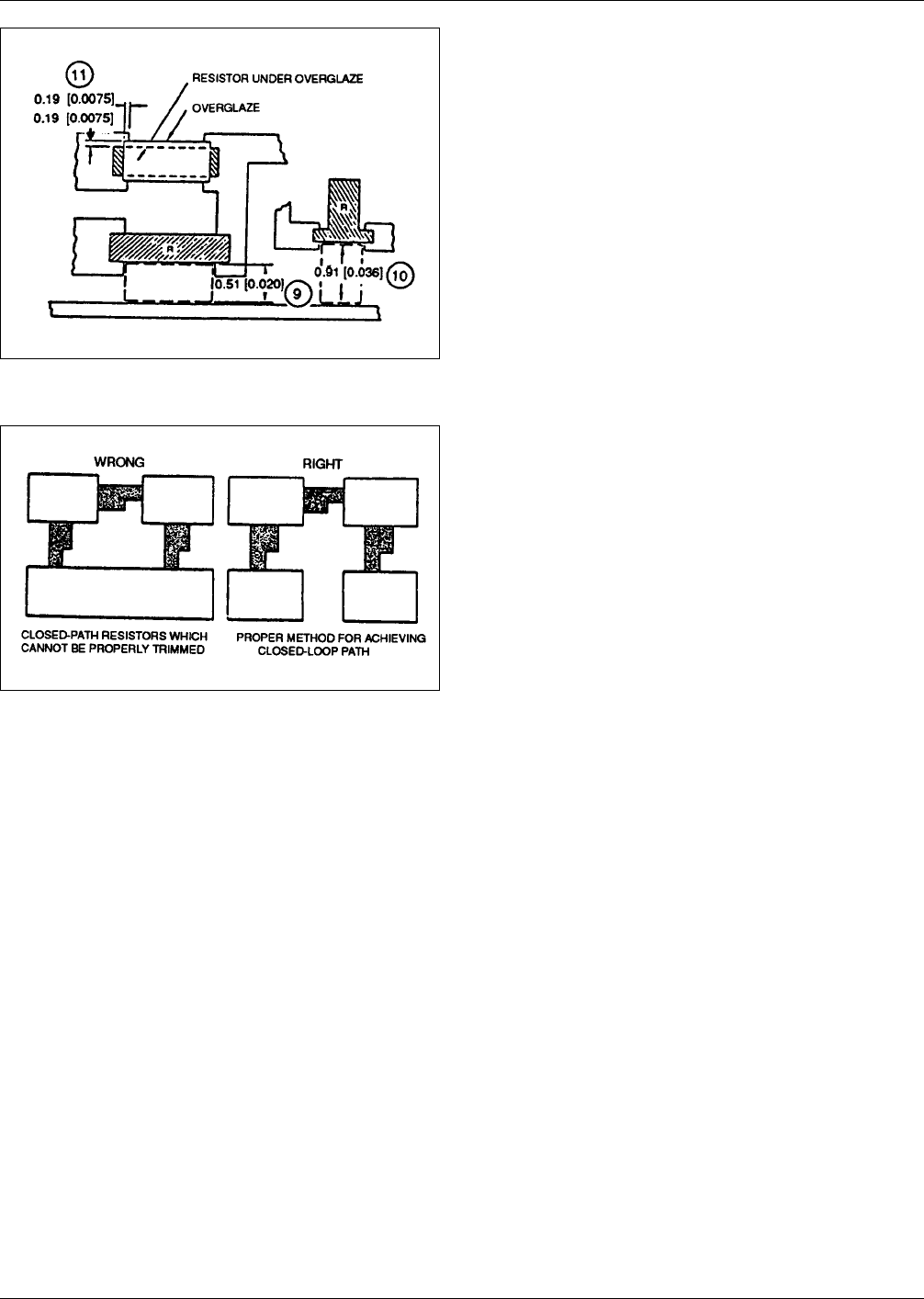
IPC-859-5-36
Figure 5–36 Nominal thick-film resistor dimensions for
trimming and overglazing (see Table 5–5)
IPC-859-5-37
Figure 5–37 Closed resistor loops
IPC-D-859 December 1989
58