IPC-D-859.pdf - 第44页
depends on the application. However , these parameters should be clearly defined on the procurement document for these parts. For optimum board design ef f iciency , the bus bar terminals should interface with the circuit…
In either case, if the assembly is to encounter a great deal
of vibration or shock, additional mechanical support should
be provided.
4.6 Special Wiring
4.6.1 Jumper Wires
It may be necessary to add point-
to-point wiring to a hybrid. Such wiring shall beconsidered
as not being part of the hybrid circuit, but as part of the
assembly process. Therefore, their use shall be documented
on the hybrid circuit master drawing.
4.6.1.1 Types Point-to-point (jumper) wires are usually
of the following types:
A. Bare bus wire that consists of a single strand of wire
that is of sufficient cross-section to be compatible with
the electrical requirements of the circuit without the use
of sleeving or other insulation.
B. Sleeved bus wire that consists of a single-strand of bare
bus wire (see A above) that is covered by insulation
tubing
C. Insulated bus wire that consists of a single strand wire
that has its own insulation when purchased, either a
plastic or varnish coating.
D. Insulated stranded wire that consists of multiple strands
of wire that are purchased with a plastic coating
4.6.1.2 Application The use of jumper wires should
adhere to the following rules:
A. Bare bus wires should not be longer than one inch.
B. Bare bus wires should not cross over hybrid conduc-
tors.
C. Bend radii for jumper wires should conform to that of
normal component bend requirements (see 4.1.11).
D. The shortest path of jumper routing should be used
unless hybrid design considerations dictate otherwise.
E. Sleeving should be of sufficient length to ensure that its
slippage at either end of the jumper wire will not result
in a gap between the insulation and solder joint or wire
bend of more than 3.2 mm [0.125 inch]. Also, the
sleeving should not be damaged by the jumper wire or
hybrid circuit soldering operations.
4.6.2 Bus Bars Bus bars are usually preformed compo-
nents in the hybrid circuit assembly that provide most, if
not all, of the power and ground distribution over the cir-
cuit surface. They are used primarily to minimize power
and ground distribution circuitry or to provide power and
ground distribution not provided by the hybrid circuit.
The number of conductor levels in the bus bar, the type and
number of their terminals, the size and finish of their con-
ductors, and the dielectric strength of the insulation
Table 4–1 Chip Carrier Application Considerations
Consideration Leadless CC’s Leaded CC’s
Thermal expansion to match P/I structure Critical Less critical
Removal and replacement Comparatively easy with special tools.
Less risk of damaging P/I
Solder joint inspection Difficult Less difficult
Flux removal after soldering Difficult Less difficult
Socket compatible Yes (except Type C) Yes (except Type B)
Lead length (CC-land pattern) Minimal Moderate (inductance greater)
Conductive cooling Good, with direct head conduction path
(Lower profile height)
Preparation for soldering Solder coating of terminals required None except for solder coating as required
for solderability
Self centering Usually Rarely
Flexure of P/I structure Critical Less critical
IPC-859-4-10
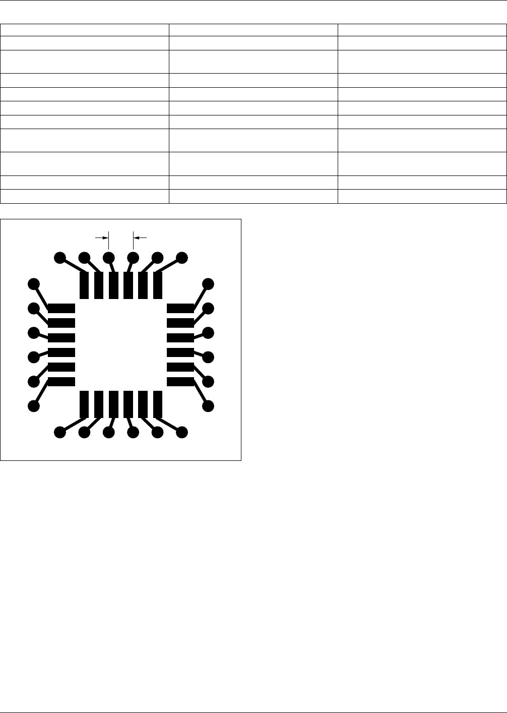
Figure 4–10 24-I/O, 1.02 mm [0.040 inch] pitch, fan-out
pattern on a custom grid
2.0
[0.080]
December 1989 IPC-D-859
37
depends on the application. However, these parameters
should be clearly defined on the procurement document for
these parts.
For optimum board design efficiency, the bus bar terminals
should interface with the circuit on a uniform termination
pattern.
4.6.3 Flex Cable When flexible cable becomes part of a
hybrid circuit assembly the terminations shall be accom-
plished in the manner that imposes no undue stress on the
cable/assembly interconnection.
IPC-859-4-11
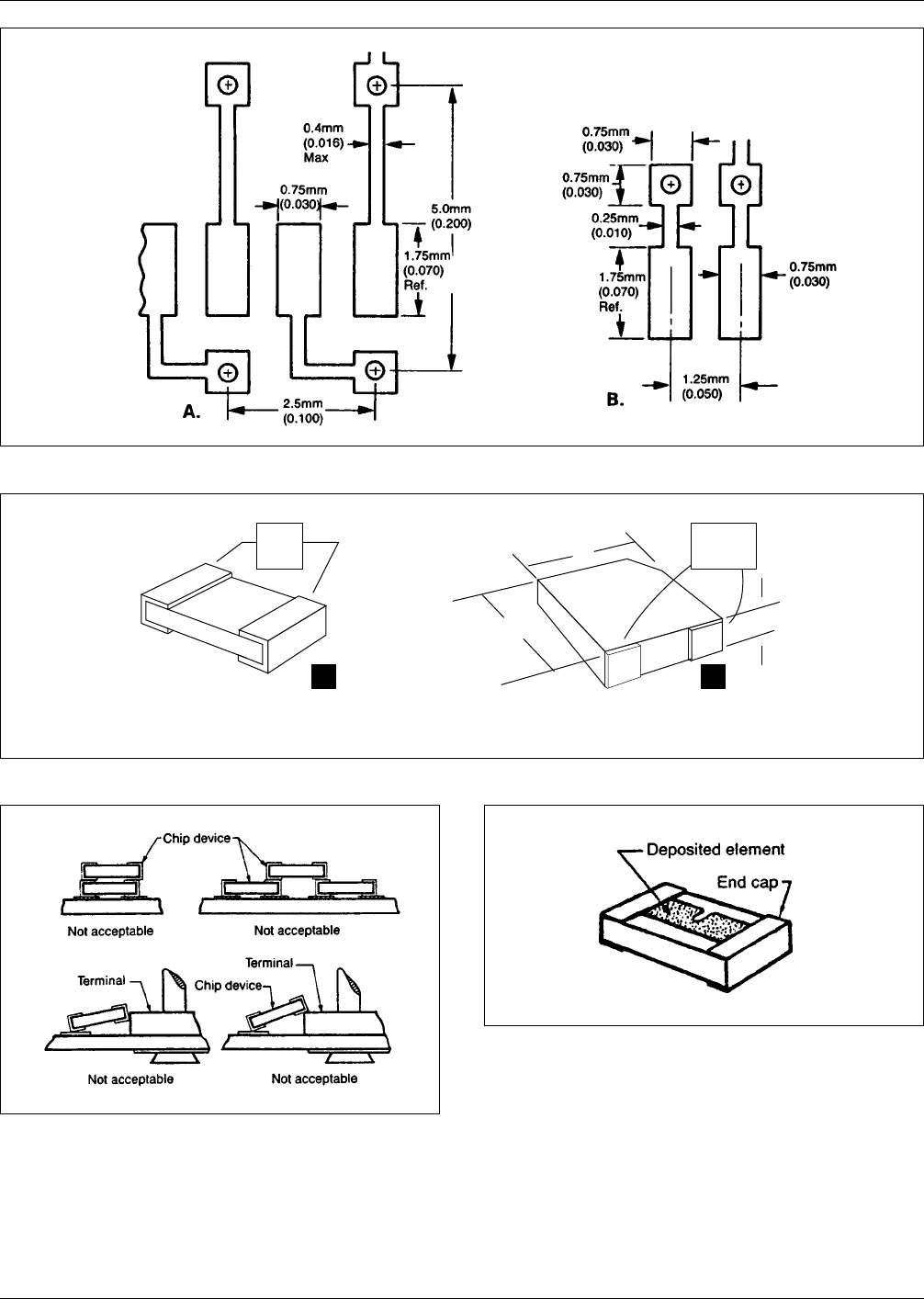
Figure 4–11 Modified fan-out patterns
IPC-859-4-12
Figure 4–12 Leadless discrete components
T
▼
▼
▼
▼
B. Reflow ConfigurationA. End Cap Configuration
A B
Reflow
Terminal
Area
End
Cap
▼
▼
W
V
▼
▼
▼
▼
IPC-859-4-13
Figure 4–13 Improper mounting of end-cap discrete
components
IPC-859-4-14
Figure 4–14 Chip resistor with deposited element
IPC-D-859 December 1989
38
Sometimes this interconnection uses pins, where a pin
passes through the substrate and the flex cable to provided
the proper interconnection. At other times, the flex cable
may be surface soldered directly to land patterns on the
hybrid circuit. Proper mechanical support, using tie-down
bars, or adhesives, shall be used to prevent stresses on the
solder joints.
5.0 Hybrid Circuit Design Requirements There are
design and documentation feature requirements that apply
to the basic layout, the artwork master, the hybrid circuit
itself, and the end-item hybrid circuit assembly. All must
be taken into consideration during the design. Therefore, it
is important to understand the relationships they have with
one another as shown in Fig. 5–1.
5.1 Design/Fabrication Sequence
5.1.1 Schematic/Logic Diagram
The initial schematic/
logic diagram designates the electrical functions and inter-
connectivity to be provided by the hybrid circuit and its
assembly. The schematic should define, when applicable,
critical circuit layout areas, shielding requirements,
grounding and power distribution requirements, the alloca-
tion of test points, and any preassigned input/out connector
locations. Schematic information may be generalized as
hard copy or computer data (manually or automated).
5.1.2 Parts List The initial Parts List should contain the
following:
A complete description of the part, quantities, manufactur-
er’s name, reference designators, and, if required, special
ordering instructions. Sometimes it is desirable to also
include the cost of the items to be used for cost analysis
purposes. The method of how the information is to be for-
matted and what must be included depends upon the stan-
dards established by each user. It is advisable to group
like-items, e.g., resistors, capacitors, integrated circuits,
etc., in some sort of ascending or numerical order. This is
of particular value to someone who must order the materi-
als.
The parts list must also have some sort of drawing number,
depending upon the design facilities system. And, in most
cases, the name of board for which it was prepared.
Included also should be the names of the persons prepar-
ing, checking, and approving this document.
Some means of identifying the revision level must also be
provided.
5.1.2.1 Non-standard Part Information When non- stan-
dard parts are used in the design, the detailed mechanical/
physical description, shall be provided as a minimum. This
information should be referenced to the schematic, so that
the appropriate layout configuration can be determined.
When non-standard parts are used, usually a specification
control drawing is required, to ensure that future parts
match the layout concepts.
5.1.3 End-product Requirements The end-product
requirements, as defined in IPC-HM-860, should be known
during the design phase. In addition, the maintenance mis-
sion of the equipment is important information to insure
the correct design approach of component placement and
conductor routing.
5.1.4 Testing Requirements Normally, prior to starting
a design, a testability review meeting should be held. Test-
ability concerns, such as circuit visibility, circuit operation,
and special test requirements and specification are dis-
cussed as a part of the test strategy. Any artwork or con-
figuration concepts necessary to test the board, shall be
incorporated into the final board layout.
During the design testability review meeting, tooling con-
cepts are established, and determinations are made as to the
most effective tool-cost versus board layout concept condi-
tions.
IPC-859-4-15
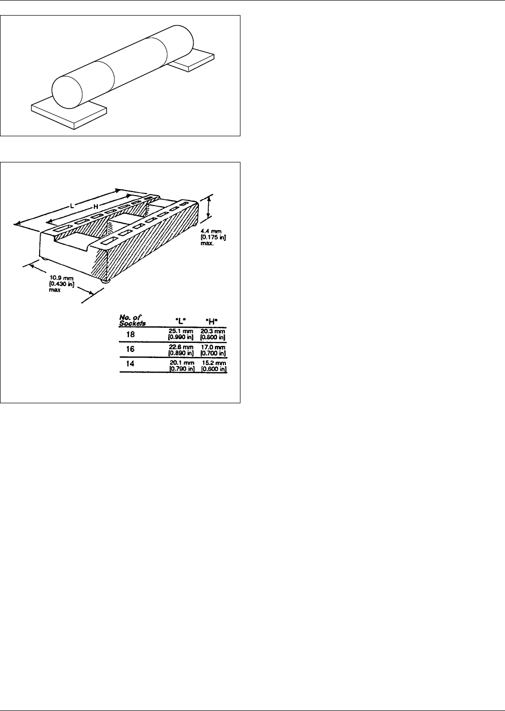
Figure 4–15 Metal electrical face (MELF) chip resistor
IPC-859-4-16
Figure 4–16 Dip socket
December 1989 IPC-D-859
39