IPC-D-859.pdf - 第71页
evaluate via resistivity . V ias are on 1.0 mm [0.040 in.] cen- ters with interconnecting conductors 0.10 mm [0.004 in.] wide. V ia size should be typical of that used on the parts in the lot. 6.5.5.8 Coupon H This coupo…
A. Part number and revision letter
B. Part traceability or lot number
6.5.4 Number of Layers The number of layers of each
coupon shall be the same as the number of layers in the
associated end-product hybrid circuit.
6.5.5 Test Coupon Examples For Quality Conformance
Testing
6.5.5.1 Coupon A
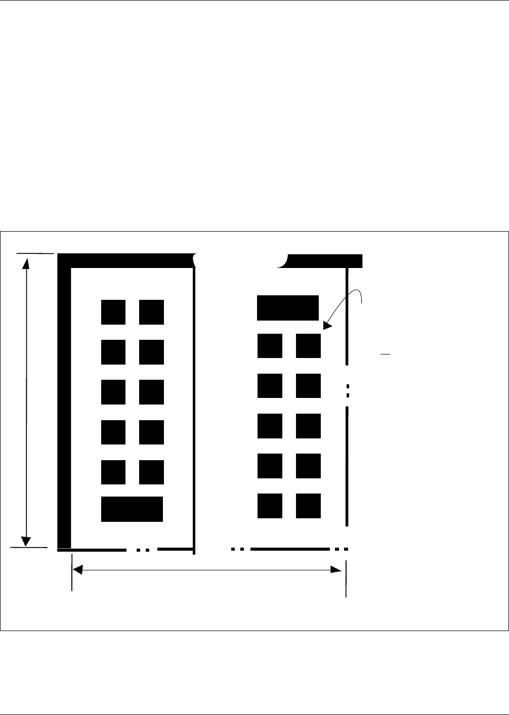
This coupon (Figure 6–2) is used to
evaluate bondability, weldability, solderability, and shorts.
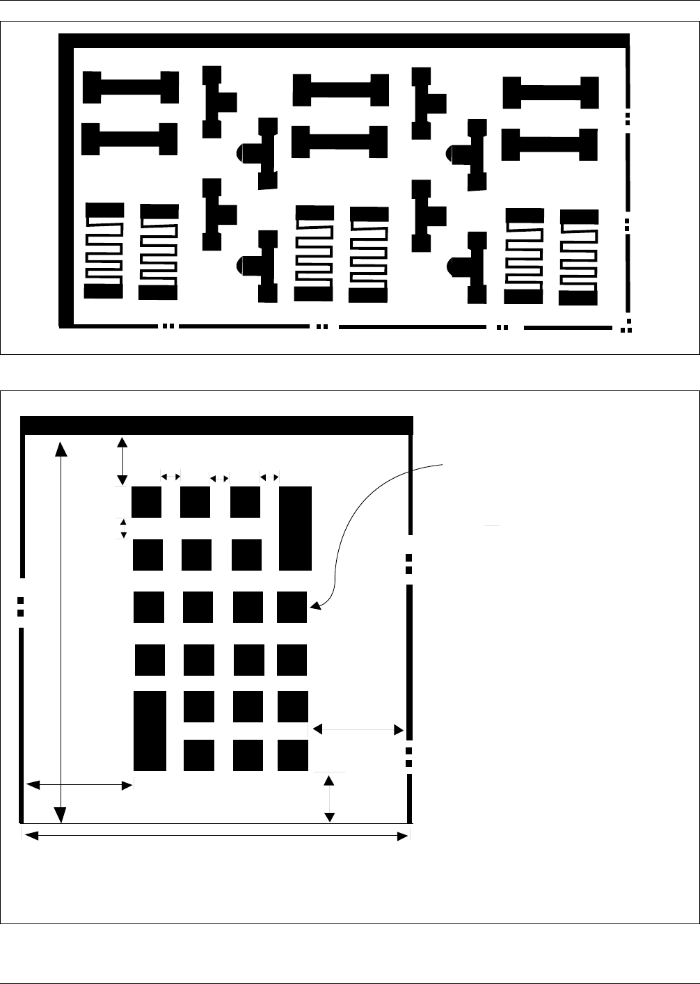
6.5.5.2 Coupon B This coupon (Figure 6–3) is used to
evaluate adhesion, passivation, dielectric resistance, and
outgassing.
6.5.5.3 Coupon C This coupon (Figure 6–4) is used to
evaluate circuit continuity, temperature cycling, thermal
cycling, and construction integrity.
6.5.5.4 Coupon D This coupon (Figure 6–5) is used to
evaluate dielectric withstanding voltage and outgassing.
6.5.5.5 Coupon E This coupon (Figure 6–6) is used to
evaluate insulation resistance. Figure 6–7 shows individual
layer artwork configuration for up to a 10-layer board.
Additional layers may be added as required.
6.5.5.6 Coupon F This coupon (Figure 6–8) is used to
evaluate resistance to electromigration. While it is designed
primarily for tests on surface layers, it may be adapted for
modified inner layer testing by the addition of vias to the
access lands at each end of the pattern.
Conductor lines are 0.10 mm [0.004 in.] with a 0.15 mm
[0.006 in.] line spacing. Test conditions, 20VDC, for 20
minutes under a drop of DI water.
6.5.5.7 Coupon G This coupon (Figure 6–9) is used to
IPC-859-6-1
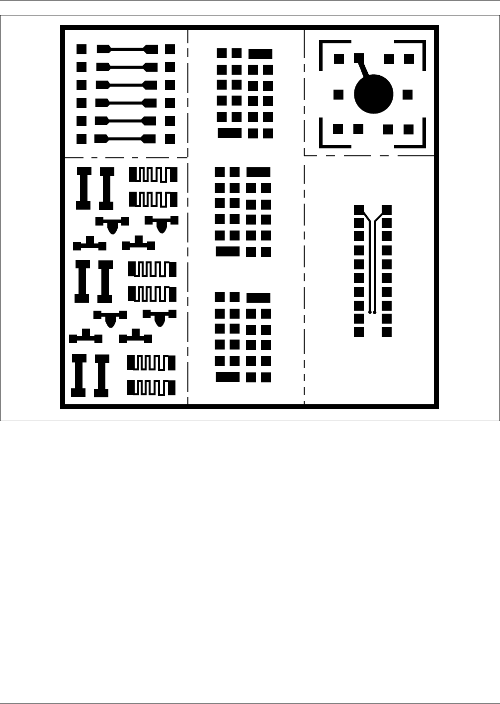
Figure 6–1 Layer 1—Individual coupon layout
IPC-D-859 December 1989
64
evaluate via resistivity. Vias are on 1.0 mm [0.040 in.] cen-
ters with interconnecting conductors 0.10 mm [0.004 in.]
wide. Via size should be typical of that used on the parts in
the lot.
6.5.5.8 Coupon H This coupon (Figure 6–10) is used to
evaluate capacitance and current density. Pattern is 10
square millimeters [0.0015 square inches].
6.5.5.9 Coupon J This coupon (Figure 6–11) is used to
measure conductor resistivity on a dielectric. Pattern is 200
squares long, printed on two layers of dielectric.
6.5.5.10 Coupon K This coupon (Figure 6–12) is used to
evaluate conductor resistivity on a substrate. Pattern is
same as Coupon J, except it is printed directly on the sub-
strate.
6.5.5.11 Coupon L This coupon (Figure 6–13) is used to
evaluate fine line resistivity. Pattern is 200 squares long,
printed on dielectric.
Figures 6–14 through 6–17 show test circuit configuration
for top and bottom layers, insulation layer, and via fill
layer.
6.5.6 Added Test Circuitry When additional testing is
desired for via tests, capacitance testing, or conductor resis-
tivity, the artwork shown in Figures 6–18 through 6–20
may be used. These need not be included in the master
drawing artwork.
IPC-859-6-2
Figure 6–2 Test Coupon A (Layer 2)
W
16 mm [0.630 in]
L
Land size:
2.0 x 2.0 mm [0.079 in x 0.079 in]
square (Typ.)
L = ( )= 2.5 mm [0.098 in]
Nr = No. of layers (Even Nos.)
= No. of layers + 1 (Odd Nos.)
Nr 3.5 mm
2 [0.138in]
x
December 1989 IPC-D-859
65
IPC-859-6-3
Figure 6–3 Test Coupon B (Layer 1)
IPC-859-6-4
Figure 6–4 Test Coupon C (Layer 2)
1.5 mm
[0.059 in]
1.5 mm
[0.059 in]
1.5 mm
[0.059 in]
W=12mm [0.470 in]
1.5 mm
[0.059 in]
1.0 mm [0.040 in] (TYP. 3 Pl.)
2.0 mm
[0.079 in]
(Typ. 4Pl.)
Land size: 1.5 x 1.5 mm
[0.059 x 0.059 in] square
(Typ.)
L = ( ) +
[0.118in]
Nr 3.5 mm
Z [0.138in]
x
3.0 mm
Nr = No. of Layers (Even Nos.)
= No. of Layers + 1 (Odd Nos.)
IPC-D-859 December 1989
66