IPC-D-859.pdf - 第15页
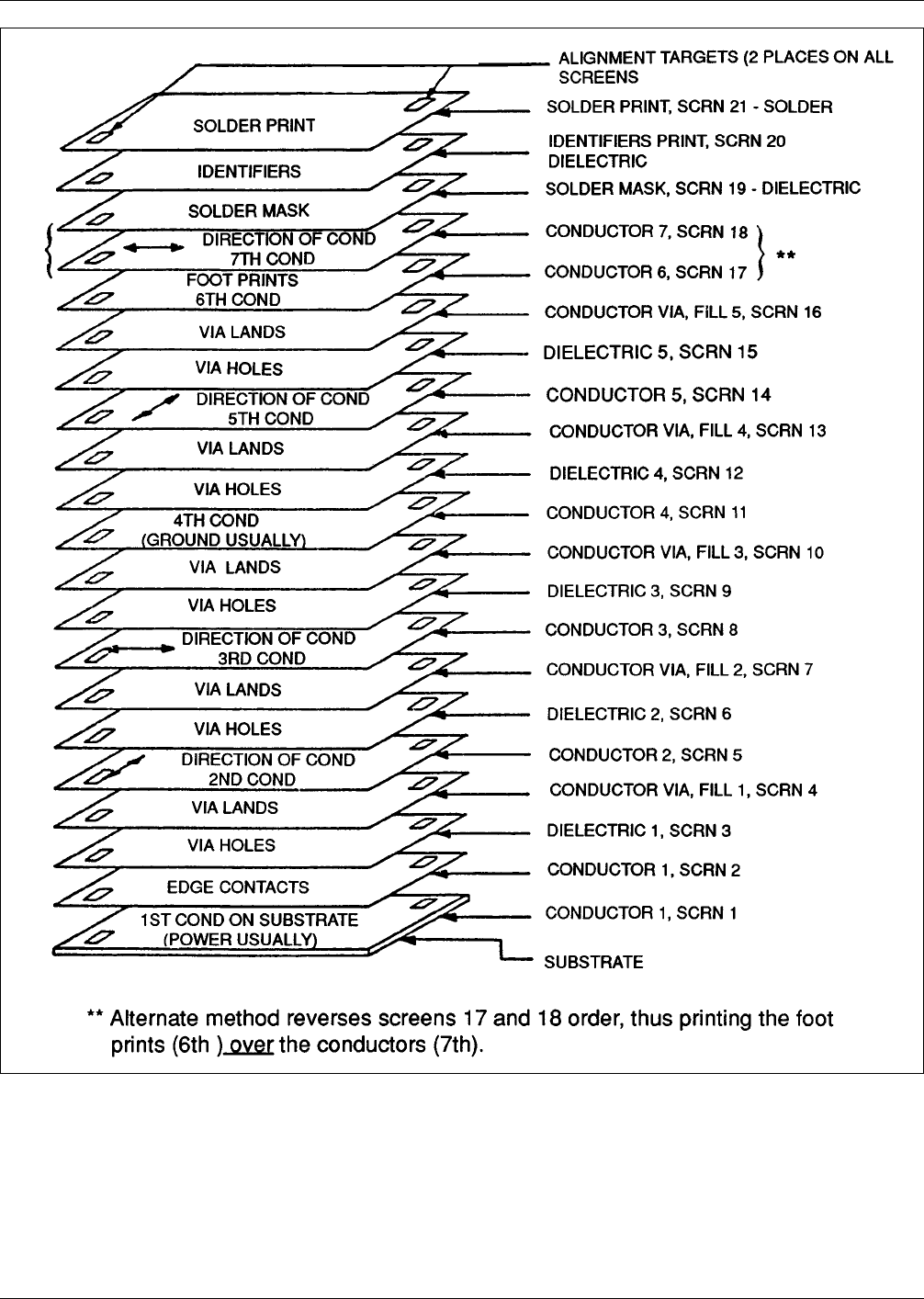
Plane sequences should be arranged so that the signal lay- ers are symmetrical about the ground or voltage plane. This may be accomplished several ways provided that any adja- cent signal layers, not separated by a groun…
typically transmitted in a mode such that all the energy is
propagated in the direction of the electric field and none in
the direction of the magnetic field.
Figure 3–7 illustrates the electric field and typical param-
eters involved in microstrip design.
When the conductor is covered with a dielectric material
such as solder mask (embedded microstrip), the impedance
characteristics will be reduced depending on the thickness
and dielectric constant of the material (approximately 5
percent).
IPC-859-3-1
Figure 3–1 Screening masks typically required for thick film processing
IPC-D-859 December 1989
8

Plane sequences should be arranged so that the signal lay-
ers are symmetrical about the ground or voltage plane. This
may be accomplished several ways provided that any adja-
cent signal layers, not separated by a ground or voltage
plane must have their key axes running perpendicular to
each other. (see Figure 3–1).
DC power and ground planes also function as AC reference
planes. Power and ground connector pins should be evenly
distributed along the edge of the board for AC reference.
3.4.3.1 Capacitance Considerations The capacitance
associated with a single crossover (see Figure 3–8) is very
small and is typically a fraction of a picofarad. As the
number of crossovers per unit length increases, the intrin-
sic capacitance of the transmission line also increases. The
crossover lumped capacitance adds to the intrinsic line
capacitance. Crossover capacitance may be approximated:
C(pF)=5.72 E
r
(l + 0.8h)
(W + 0.8h)
h
provided that l ≥ 0.5h
W ≥ 0.5h
Where:
E
r
= dielectric constant
h = dielectric thickness between crossovers
(mm)
l = length (mm)
W = width (mm)
The distributed coupling capacitance between two parallel
conductors on the same layer (see Figure 3–9), assuming
0.015 mm [0.0006 inch] print thickness, is given by
C
C
=
N
∑ 6.7x10
–4
l
n
d
n
pF
n = 1
Where: l
n
= length of parallelism between the conduc-
tors
for separation d
n
d
n
= perpendicular distance between
the conductors
The above equation is a first order approximation which
disregards capacitance contributed by all other conductors
distributed across the entire substrate. It is assumed that the
first order contributions constitute 90% or more of the cou-
pling capacitance, and that coupling between adjacent con-
ductors is the prime concern.
Circuit design shall specify the allowable capacitances
from which the required spacing and maximum parallelism
shall be determined.
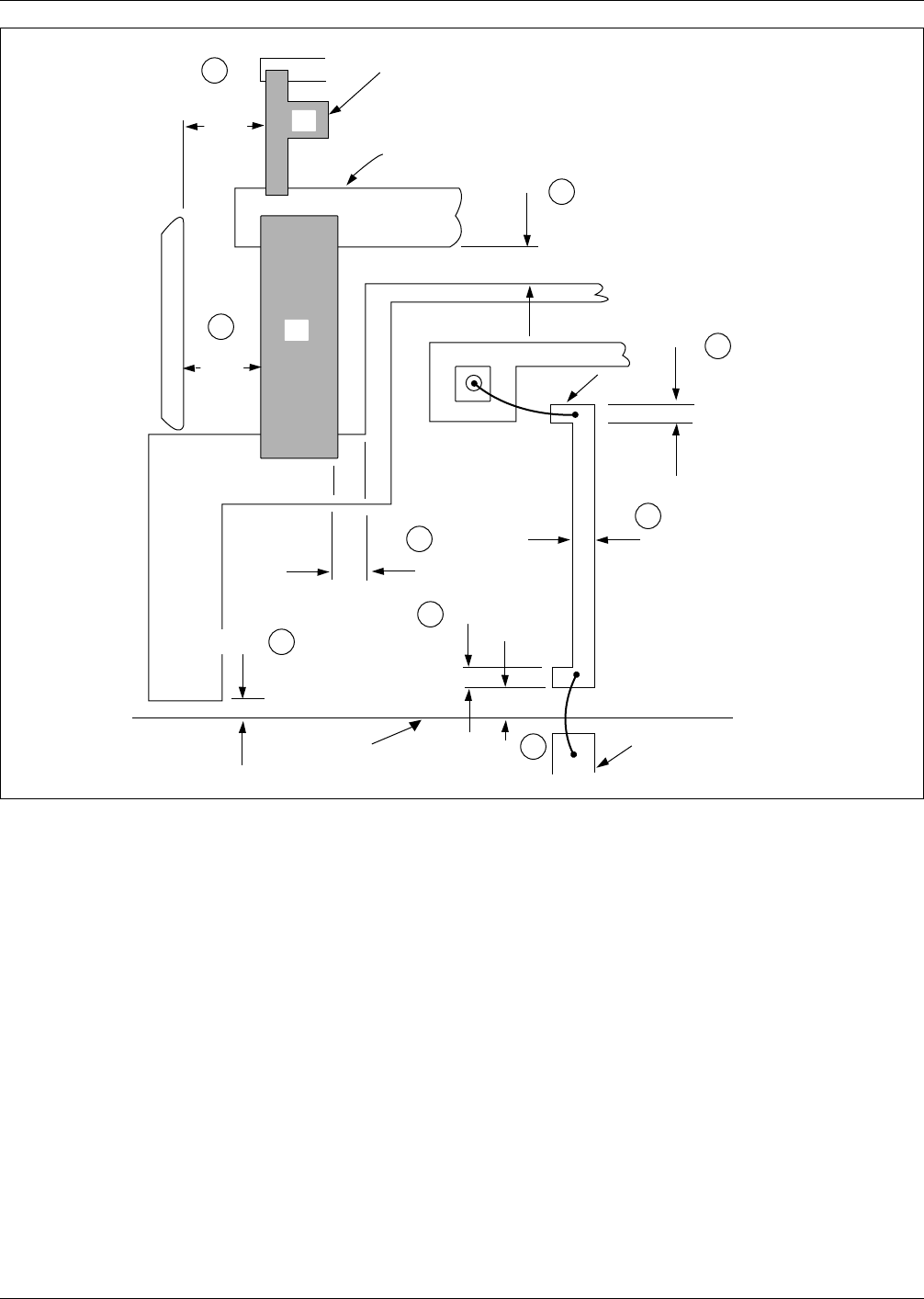
Table 3–1 Dimensional Constraints for Thick-Film Conductors and Lands
Conductor and Land Sizes and Spacing
Minimum
Dimension
mm [inch]
Nominal
Dimension
mm [inch]
Maximum
Dimension
mm [inch] Figure Item
Conductor to edge of substrate for conductors
≤0.38 mm [0.015 inch]
0.25 [0.010] 0.51 [0.020] None 3–2
1
Conductor to edge of substrate for conductors
>0.38 mm [0.015 inch]
0.25 [0.010] 0.32 [0.0125] None 3–2
2
Exit bonding lands (width and length) 0.25 [0.010] 0.32 [0.0125] None 3–2
3
Wire bonding lands (width and length—one or two
wires on same land) (preferred)
0.25 [0.010] 0.32 [0.0125] None 3–2
4
Wire bonding lands (width and length—one wire per
land (special)
0.25 [0.010] 0.32 [0.0125] None 3–3
5
Conductor width (preferred) 0.25 [0.010] 0.51 [0.020] None 3–2
6
Conductor width (special) 0.13 [0.005] 0.25 [0.010] None 3–3
7
Conductor-to-conductor spacing (preferred) 0.25 [0.010] 0.51 [0.020] None 3–2
8
Conductor-to-conductor spacing (special) 0.13 [0.005] 0.25 [0.010] None 3–3
9
Conductor-to-resistor spacing (on untrimmed
side of resistor)
0.25 [0.010] 0.38 [0.015] None 3–4
10
Conductor-to-resistor spacing (on trimmed side of
resistor)
0.38 [0.015] 0.51 [0.020] None 3–4
11
Conductor-to-resistor spacing, top-hat configuration 0.76 [0.030] 0.89 [0.035] None 3–2
15
Upper and lower conductor widths at crossover junc-
tion
0.25 [0.010] 0.38 [0.015] None 3–4
12
Crossover conductor-to-connecting-conductor
overlap-length
0.25 [0.010] 0.32 [0.0125] None 3–4
13
Conductor crossover dielectric overlap 0.25 [0.010] 0.38 [0.015] None 3–4
14
Dielectric to resistor spacing 0.51 [0.020] 0.51 [0.020] None 3–4
16
December 1989 IPC-D-859
9
3.4.4 Power Distribution Considerations Power distri-
bution is important in the design of a multilayer hybrid cir-
cuit. The grounding scheme, as a part of the distribution
system, provides not only a DC power return, but also pro-
vides an RF return plane for digital logic to be referenced.
In a typical multilayer design, a combination power/ground
plane is screened directly on the substrate. Vias for the
power and ground connections are often made larger than
the vias for signal interconnection because the power and
ground connection vias carry more power and they traverse
more layers. Above this are alternate layers of dielectric
and interconnect metallization.
The top layer contains all device I/O bonding lands and the
substrate I/O lands. If space permits, this layer may also
contain some interconnections.
Metallization lands are provided for physical attachment of
the integrated circuit chips. These lands are normally con-
nected to ground or a voltage supply. Eight metallization
layers are generally considered to be a reasonable maxi-
mum. The base metal in coated metal-core substrates may
be utilized as a ground plane that is contacted directly by
printing a circuit directly over a via through the coating.
The following items should be taken into consideration:
1. Maintain a lower RF impedance throughout the DC
power distribution. An improperly designed ground
can result in RF emissions as a result of radiated field
gradients developed across the uneven circuit imped-
ance, and its inability of decoupling capacitors to effi-
ciently reduce the EMI.
2. Decouple the power distribution at the hybrid circuit
connector using a 1.0 to a 10.0 microfarad tantalum
capacitor.
3. A ceramic capacitor of approximately 0.01 microfarads
should be connected across VCC or source voltage;
IPC-859-3-2
Figure 3–2 Nominal thick film conductor and land dimensional constraints (see Table 3–1)
TOP HAT
CONFIGURATION
CONDUCTOR
15
8
4
11
10
2
3
6
1
0.91
[0.036]
R
0.51
[0.020]
0.32
0.0125
0.41
[0.016]
0.32
[0.0125]
0.51
[0.020]
0.32
[0.0125]
0.51
[0.020]
Bonding
Pad
CR
R
0.51
[0.020]
EDGE OF
SUBSTRATE
LEAD
DIMENSIONS
IN mm [inches]
IPC-D-859 December 1989
10