IPC-D-859.pdf - 第24页
and electrical connections. This support should also be suf- ficient to help prevent cracking or loosening of conductors, breaking of part leads or wire bonds, or cracking or chip- ping of the substrate resulting from flex…
where R = thermal resistance of the material layer
(°C/W)
t = thickness of the material layer (mm)
K = thermal conductivity of the material
in (W/°C–mm)
A = cross-sectional area of the material
layer (mm
2
)
Table 3–3 gives the thermal conductivity of typical materi-
als used in hybrids.
Heat spreading occurs when heat flows into a material
layer of increased cross-sectional area. As illustrated in
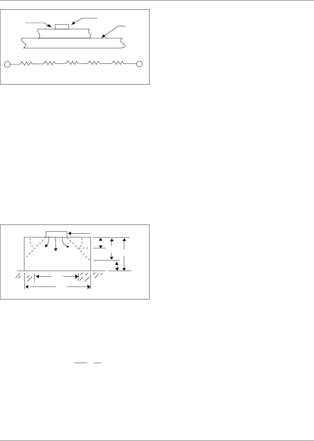
Figure 3–14 it is adequate to assume that spreading occurs
at a 45 degree angle.
To calculate thermal resistance when heat spreading
occurs, the average cross-sectional area should be used
over the range of spreading. As shown in Figure 3–13 the
total thermal resistance (R
T
) will be:
R
T
= R
1
=
1/2t
1
KA
1
+
t
2
Ka
Notes: 1. Use average area A over thickness 1/2t
1
. 2. Use area A
over thickness t
2
. 3. No spreading occurs over t
2
.
To the maximum extent possible, devices dissipating sig-
nificant amounts of power should be spaced in the hybrid
in such a manner as to spread the heat flow throughout the
case. When devices are close enough that their areas of
heat spreading overlap, based on the 45 degree assumption,
their thermal interaction should be taken into account. This
can be done by limiting the cross-sectional area used in the
thermal-resistance calculations to areas that do not overlap
the heat spreading of other devices.
When device power dissipation becomes significant, steps
may be taken to minimize the temperature rise. Devices
may be eutectically mounted directly to the substrate or to
ceramic, molybdenum, or kovar ‘‘tabs’’ to increase heat
spreading and to reduce thermal resistance. In extreme
cases, but at considerable cost, devices can be mounted on
Beryllia substrates or metal heat-sinks.
Note that in the above discussion the temperature rise is
related to the hybrid case temperature, not to the ambient
air or to the hybrid mounting surface. The hybrid case tem-
perature will in turn be a function of the ambient air and
mounting surface temperature, the thermal properties of the
mounting surface, and the hybrid to mounting surface inter-
face.
3.5.5 Thermal Matching A primary thermal concern
with ceramic surface-mounted components is the thermal
expansion mismatch between the component and the sub-
strate. This mismatch may result in fractured solder joint
interconnections if the assembly is subjected to thermal
shock, thermal cycling, power cycling and high operating
temperatures. The number of fatigue cycles before solder
joint failure is dependent on, but not limited to, the thermal
expansion mismatch between the component and the sub-
strate, the delta temperature excursion over which the
assembly must operate, the solder joint size, the size of the
component, and the power cycling that may cause an unde-
sirable thermal expansion mismatch if a significant tem-
perature different exists between the component and the
substrate.
With surface-mount components, the number of fatigue
cycles can be increased by reducing the thermal expansion
mismatch, reducing the temperature gradient, increasing
the height of the solder joint, using the smallest physical
size component wherever possible, and by optimizing the
thermal path between the component and the substrate.
3.6 Mechanical Requirement Considerations
3.6.1 Camber
All multilayer hybrids will warp to some
degree unless rigidly supported along all edges. The con-
struction of the board should be as symmetrical as possible
with respect to conductor area distribution and to a lesser
degree, the amount of dielectric applied in which there
exists a Coefficient of Thermal Expansion (CTE) mismatch
between the dielectric and the supporting substrate. Warp-
ing is more likely to occur on the boards having large
width-to-length ratios and in boards having large conductor
areas on one side.
3.6.2 Support All hybrid circuit assemblies should be
supported in order to minimize stress on the components
IPC-859-3-13
Figure 3–13 Example of total thermal resistance
calculation
Mounting
Material
Electrical Device
Substrate
Hybrid
Case
Mounting
Material
Mounting
Material
Electrical
Device
Mounting
Material
Substrate
Hybrid Case
R
R
RRR
5
4
3
2
1
IPC-859-3-14
Figure 3–14 Thermal resistance during heat spreading
ELECTRICAL DEVICE
Heat
45°
45°
A
A
1
t
t
1
1/2 t
1
t
2
December 1989 IPC-D-859
17

and electrical connections. This support should also be suf-
ficient to help prevent cracking or loosening of conductors,
breaking of part leads or wire bonds, or cracking or chip-
ping of the substrate resulting from flexing stress on the
assembly.
3.6.3 Shock and Vibration The ultimate ability of com-
ponents to survive shock and vibration environments will
depend upon the degree of consideration given to the fol-
lowing factors
A. The worst-case levels of shock and vibration environ-
ment for the entire structure in which the hybrid circuit
assembly resides, and the ultimate level of this environ-
ment that is actually transmitted to the components.
(Particular attention should be given to equipment that
will be subjected to random vibration.)
B. The method of mounting the assembly in the equipment
to reduce the effects of the shock and vibration environ-
ment, specifically the number of mounting supports,
their interval, and their complexity.
C. The attention given to the mechanical design of the
assembly, specifically its size, shape, type of material,
material thickness, and the degree of resistance to bow-
ing and flexing that the design provides.
D. The shape, mass and location of the components
mounted on the assembly.
E. The component lead wire stress relief design as pro-
vided by its package, lead spacing, lead bending, or a
combination of these, plus the addition of restraining
devices.
F. The attention paid to workmanship during assembly, so
as to insure that component leads are properly bent, not
nicked, and that the components are installed in a man-
ner that tends to minimize component movements.
G. Conformal coating may also be used to reduce the
effect of shock and vibration on the assembly.
The selection of components to be mounted on assemblies
subjected to severe shock and vibration should favor,
where circuit design permits, the use of components that
have lightweight, low-profile packages and that have inher-
ent strain relief provisions. Where discrete components
must be used, preference should be given to axially-leaded
types that present a relatively-low profile, and that can be
mounted and easily clamped in intimate contact with the
board surface.
The use of irregularly-shaped components, especially those
having a large mass and a high center of gravity, should be
avoided where practical. If their use cannot be avoided,
they should be located toward the outer perimeter of the
assembly where the guides and/or connectors can help to
provide resistance to flexing. Depending on the severity of
this problem, the use of mechanical clamping, adhesive
bonding, or embedding may be required.
3.7 Test Requirement Considerations The circuit lay-
out configuration, uniformity of the hybrid circuit size,
shape and functional connector interface will have an effect
on the manufacturability, testability, and cost of the fin-
ished assembly. These aspects must be considered early in
the design stage of product development. Some important
test considerations are specified in the following para-
graphs.
3.7.1 Hybrid Circuit Layout Design The design layout
from one design to another should be such that designated
areas are identified by function, i.e., power supply section
confined to one area, analog circuits to another section, and
logic circuits to another, etc. This will help to minimize
cross-talk, simplify test fixture design, and facilitate
trouble-shooting diagnostics. In addition, the design
should:
• Have circuit elements placed away from the assembly
edges to allow adequate test fixture clearance.
• Have design grid layout compatible with testing plan.
• Allow provision for isolating parts of the circuit to
facilitate testing and diagnostics.
• Where practical, group test points and jumper points in
the same physical location on the circuit.
• Consider Large Scale Integrated (LSI) circuit socketing
for components so that parts can be easily replaced for
further testing.
• Consider surface mounted components and their patterns
require special consideration for test probe access.
• Allow adequate space between devices for rework
access.
• Orient devices in same direction if possible for ease of
trouble- shooting and rework.
3.8 Materials The effect that one material may have
upon another material within a hybrid is of extreme con-
cern. Therefore, contemplated material substitutions should
be reviewed to determine whether the proposed design is
susceptible to failure mechanisms.
Nonconforming materials can result in failure of the hybrid
circuit caused by one or more of the following conditions:
A. Metal migration
B. Corrosion or oxidation
C. Ionic contamination
D. Improper adhesion
E. Intermetallic formation
IPC-D-859 December 1989
18

F. Differences in thermal coefficients of expansion
G. Variations in electrical characteristics of screened com-
ponents
3.8.1 Substrates The substrate serves as the supporting
structure for the circuitry. It acts as a surface for depositing
the conductive, dielectric, and resistive materials that form
the passive circuit elements. Also, it is a base for mechani-
cal support of all active and passive chip components. It
must be an electrical insulator to isolate the various con-
ductive paths of the circuit, and it must have sufficient
thermal conductivity to remove heat generated by the cir-
cuit components. See Table 3–4 and 3–5 for substrate
selection criteria.
The material most suitable for the particular application
should be determined by examining the following proper-
ties of substrate materials:
A. Thermal conductivity—The ability of the material to
conduct heat away from critical circuit components.
Normally measured as cal–cm/sec–cm
2
–°C. High ther-
mal conductivity is desired.
B. Electrical insulation—The ability of the material to
insulate various circuit components from one another.
Normally measured in ohm/cm. High resistivity is
desired.
C. Mechanical strength—The ability to withstand
mechanical shock. Young’s modulus, flexular strength,
tensile strength, and compressive strength are consid-
ered measures of mechanical strength. High strength is
desired.
D. Refractory property—The ability of the material to
withstand high temperatures. Melting point is an indi-
cator of this property. This property is usually desir-
able, and absolutely mandatory for processes requiring
heat treatment.
E. Thermal expansion—This property is an important
consideration, especially when the structure is placed
into a metal case or mounted to an organic interconnec-
tion substrate.
F. Chemical susceptibility—The ability to withstand
exposure to chemicals. It is very desirable for sub-
strates to be inert to processing chemicals.
G. Weight—Weight may or may not be a consideration
based on the application.
H. Metallizability—The ability of the material to be suc-
cessfully metallized.
I. Cost—There are wide variations in the cost of substrate
materials.
Table 3–4 Nonphysical Substrate Selection Criteria
Material
Cost per 25 x 25 mm [1 x 1-inch] Substrate for
Applications Remarks100 5000 100K
Alumina Medium Medium Very low General Use Very popular
Beryllia High Medium Low Heat dissipating Low thermal resistance
Porcelainized
steel
Medium Low Low Special shapes Becomes cost effective
for large substrates
Cofired multilayer
ceramic
Very high High Medium Package May be cost effective
in large quantities
Table 3–5 Important Characteristics of Substrates
Material
Tensile
Modulus
MPa
Coefficient
of Thermal
Expansion
(ppm/°C)
Tensile
Strength
MPa
Thermal
Conductivity
(W/°C—mm)
Dielectric
Constant
(1 MHz)
Dissipation
Factor
Alumina (90%) 324.07 6.70 317.17 16.74 9.40 *
Alumina (96%) 324.07 7.11 317.17 25.10 9.90 0.0001–0.0002
Alumina (99.6%) 344.75 6.30 448.18 37.40 10.00 0.0001–0.0002
Aluminum
Nitride
291.66 4.30 367.50 170.00 8.80 *
Beryllia 319.93 8.00 * 250.00 7.00 0.0001
Quartz 72.40 0.72 * 0.75 3.80 0.0002
Sapphire 344.75 7.74 0.00 25.00 0.00 0.002
Porcelainized
steel
* 4.40 89.64 1.67 5.50 *
* Indicates data not available
December 1989 IPC-D-859
19