IPC-D-859.pdf - 第47页
to structure this information so that there can be no misun- derstanding for anyone viewing the layout. Notes are espe- cially important for the engineering review cycle, the digi- tizing ef fort, and when the document i…
During the layout process, any circuit board changes that
impact the test program, or the test tooling, shall immedi-
ately be reported to the proper individuals for determina-
tion as to the best compromise. The testing concept should
develop approaches that can check the board for problems,
and also detect fault locations wherever possible.
Figure 5–2 provides a Testability Design Check-list to be
used in evaluating the testability of the design.
5.1.5 Layout Concepts The final layout is used for pre-
paring artwork and for fabrication and assembly of proof-
of-design and prototype hybrids. It depicts the hybrid
microcircuit as it will actually appear after assembly with
all components located in their final positions, wire bonds
routed to the proper lands, and resistors of the proper size.
5.1.5.1 Feasibility Density Evaluation After approved
documents for the items described in 5.1.1 through 5.1.4
are provided, and before the actual drawing of the layout is
begun, a feasibility density evaluation should be made.
This should be based on the maximum size of all parts
required by the Parts List, and the space they and their
lands will require on the total circuit, exclusive of intercon-
nection conductor routing. The total circuit geometry
required for this mounting and termination of the compo-
nents should then be compared to the total usable area for
this purpose. The more reasonable the maximum values
are, the greater will be the chances for the completion of a
successful design.
5.1.5.2 Grid Systems The grid system used shall match
the requirements of the master drawing, see paragraph
3.3.3.
When component locations or other pattern features do not
end on grid, their locations are critical, and their center-
lines must be drawn or accurately defined on the layout.
5.1.5.3 Viewing The layout should always be drawn as
viewed from the component side of the board. For artwork
generation purposes, paragraph 5.5, the viewing require-
ments shall be identical to the layout. (See IPC-D-310 and
Figure 3–1).
The definition of layers of the circuit shall be as viewed in
3.3.2, with distinguishing characteristics used to differenti-
ate between conductors on different layers of the circuit.
5.1.5.4 Accuracy The drawing scale used for the layout
should be sufficiently high (usually 20:1 or 40:1) to mini-
mize inaccuracies when it is being interpreted during the
artwork generation process.
5.1.5.5 Layout Notes The layout should be completed
with the addition of appropriate notations, marking require-
ments, and revisions/status level definition. It is necessary
IPC-950-4-17
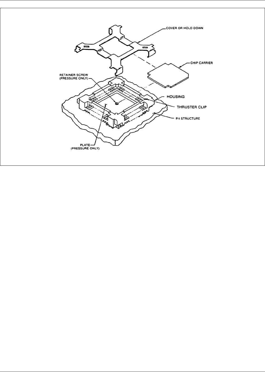
Figure 4–17 Surface mount chip carrier socket
IPC-D-859 December 1989
40
to structure this information so that there can be no misun-
derstanding for anyone viewing the layout. Notes are espe-
cially important for the engineering review cycle, the digi-
tizing effort, and when the document is used by someone
other than the originator.
5.1.5.6 Automated Layout Techniques All of the infor-
mation contained in 5.1.5 through 5.1.5.6 is applicable to
both manual and automated layout generation. However,
when automated layout techniques are used, it is also nec-
essary that they match the design system being employed.
This may include the use of computer-aided-drafting assis-
tance that primarily helps in the defining of components
and conductors, or may be as sophisticated as to add the
placement of gates, the placement of components, and/or
the routing of conductors.
When automated systems must communicate with each
other, it is recommended that standard files be used for this
technique. A standard format has been developed, such as
IPC-859-5-1
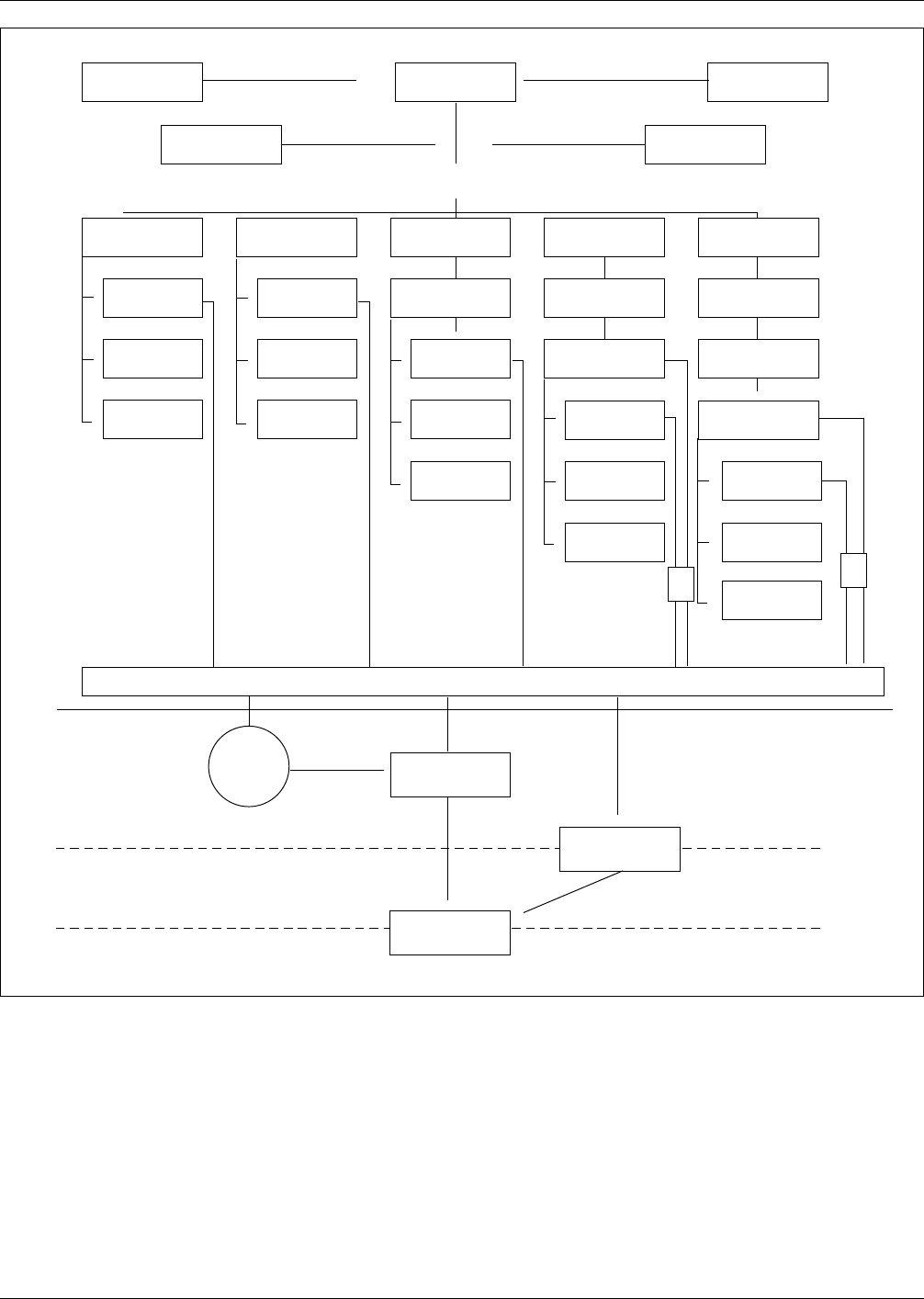
Figure 5–1 Simplified flow chart of hybrid circuit design/fabrication sequence
▼
▼
▼
▼
▼
▼
▼
▼
▼▼ ▼
▼
▼▼
▼▼▼
▼▼▼
▼▼▼
▼▼▼
▼▼
▼
▼
▼
▼▼
▼
▼▼▼▼▼
OR
OR
Assembly
Test
Hole &
Process
Data
Panel or
Printed Board
(Rigid or Flexible)
Assembly
Sequence/
Process Data
Printed
Board
Assembly
Parts
List
Schematic/Logic
Diagram
End Product
Specification
CAD
Library
Test
Coupon
Manual
Layout
Tape
Masters
Digitize for
N/C as Required
Other
Documentation
Manual
Layout, Digitize
Manual
Layout, Digitize
Input Data and
Circuit Analysis
Input Data and
Circuit Analysis
Photoplot
Masters
N/C Tape
Output
Other
Documentation
Other
Documentation
Other
Documentation
Other
Documentation
N/C Tape
Output
N/C Tape
Output
N/C Tape
Output
Interactive Edit.
and Rules Check
Batch D/A Place
and Route
Interactive Place
and Route
Photoplot
Masters
Photoplot
Masters
Photoplot
Masters
On Line or Follow
on Rules Check
Interactive Completion
In Real Time
Manual Complete
if Required
SINGLE OR MULTIPLE IMAGE PRODUCTION MASTER ORIGINALS
1-Manual 2-Manual/Digitize
3-Computer
Aided Drafting
4-Design Automation
(DA) (Batch)
5-Computer Aided Design
(CAD)--Interactive
▼
▼
▼
▼
▼
December 1989 IPC-D-859
41

the IPC-D-350 series, to facilitate the interchange of infor-
mation between automated systems.
Archiving of data shall be in accordance with IPC-D-350,
IPC- D-351, IPC-D-352, IPC-D-353 and IPC-D-354.
With automated techniques, the data base should include
the completeness of all information that will produce the
hybrid circuit. As required, this will include all notes, plat-
ing requirements, substrate thickness, etc. The use of a
check plot is important tohelp verify that the data base
matches the requirements, as necessary.
5.2 Substrate Geometries
5.2.1 Size and Shape
The size and shape of a hybrid
substrate can be of critical importance. Because of the
brittle nature of typical hybrid substrates (ceramics), care
must be exercised in both the design outline layout and
material selection.
• Route test/control points to the edge connector to enable
monitoring and driving of internal circuit functions and to
assist in fault diagnosis.
• Divide complex logic functions into smaller, combina-
tional logic sections.
• Avoid one-shots; if used, route their signals to the edge
connector.
• Avoid potentiometers and ‘‘select-on-test’’ components.
• Use a single, large-edge connector to provide I/O pins and
test/control points.
• Make PC-board I/O signals TTL-compatible to keep ATE
interface costs low and give flexibility.
• Provide adequate decoupling at the board edge and locally
at each IC.
• Provide signals leaving the hybrid with maximum fan-out
drive, or buffer them
• Buffer edge-sensitive components from the edge
connector—such as clock lines and flip-flop outputs.
• Never exceed the logic rated in-out; in fact, keep it to a
minimum.
• Avoid devices that require high-fan-outs.
• Keep logic depth on any hybrid to a low level by using
edge-terminated test/control points.
• Single-load each signal entering the hybrid whenever pos-
sible.
• Terminate unused logic pins appropriately to minimize
noise pick-up.
• Do not terminate logic outputs directly into transistor
bases. Do use a series current-limiting resistor.
• Buffer flip-flop output signals before they leave the
hybrid.
• Use open-collector devices with pull-up resistors to
enable external override control.
• Avoid using redundant logic to minimize undetectable
faults.
• Bring outputs of cascaded counters to higher-order
counters so that they can be tested without large counts.
• Construct trees to check the parity of selected groups of
eight bits or fewer.
• Avoid wire-OR and wire-AND connections. If you can’t,
use gates from the same IC package.
• Provide some way to bypass level-changing diodes in
series with logic outputs.
• Break paths when a logic element fans out to se veral
places that converge later.
• Use elements in the same IC package when designing a
series of inverters or inverters following a gate function.
• Standardize power-on and ground pins to avoid test-
harness multiplicity.
• Bring out test points as near to d/a conversions as pos-
sible.
• Provide a means of disabling on-board clocks so that the
tester clock may be substituted.
• Provide mounted switches and RC networks with over-
ride lines to the edge connector.
• Route logic drives of lamps and displays to the edge con-
nector so that the tester can check for correct operation.
• Separate analog circuits from digital logic, except for tim-
ing circuits.
• Uniformly mount ICs and clearly identify them to make it
easier to locate them.
• Provide sufficient clearance around IC sockets and direct-
soldered ICs so that IC clips can be attached whenever
necessary.
• Add top-hat connector pins or mount extra IC sockets
when there aren’t enough edge-connector pins for test/
control points.
• Use sockets with complex ICs—CPUs, UARTs, and long,
dynamic shift registers.
• Wire feedback lines and other complex circuit lines to an
IC socket with a jumper plug so that they can be inter-
rupted at test.
• Use jumpers that can be cut during debugging. The jump-
ers can be located near the connector.
• Fix locations of power and ground lines for uniformity
among several hybrid types.
• Make the ground trace large enough to avoid noise prob-
lems.
• Group together signal lines of particular families.
• Clearly label all parts, pins, and connectors
Figure 5-2 Testability design checklist
IPC-D-859 December 1989
42