IPC-D-859.pdf - 第58页
5.3.3.2 Automatic Bonding All the requirements ofmanual wire bonding apply to automatic bonding with the following exceptions: A. W edge bonds —W edge bonds shall be made only to gold metallization. B. Substrate refer en…
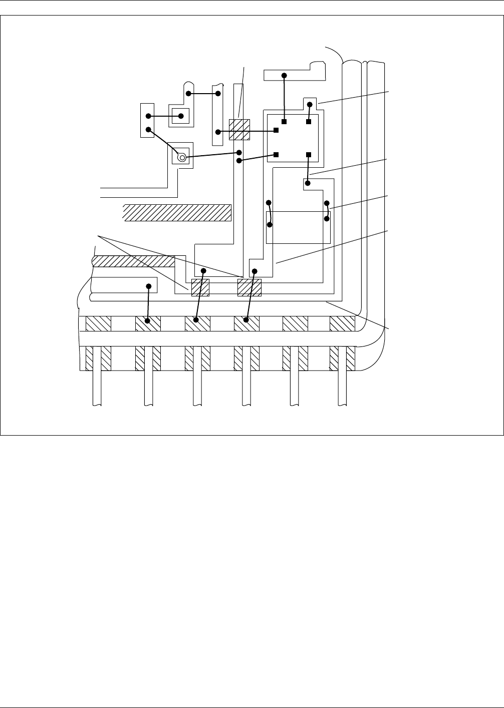
metallizations, the conductor metal shall be covered with-
protective dielectric to prevent sagging wire bonds from
causing catastrophic failure. Figure 5–28 illustrates
examples of this principle.
5.3.3.1 Manual Bonding The following should be con-
sidered if manual wire bonding is utilized.
A. Wire types—Minimum manual-bonding wire size
should be checked to ensure sufficient current-carrying
capacity. See Table 5–2.
Due to the small (0.076 to 0.127 mm [0.003 to 0.005
inch]) size of the bonding lands on transistors and
diode chips 0.178 mm [0.007 inch] diameter, wires can
be used for manual wire bonding of these devices, how-
ever, the designer should provide the largest possible
mounting and bonding lands on the substrate. This not
only facilitates initial bonding, but provides room for
the making of additional bonds should the device need
to be replaced or repaired. Use of 0.025 mm [0.001
inch] diameter wire is preferred.
B. Wire bond parallelism—Wire bonds should parallel
the substrate edge if possible.
C. Wire length—Maximum and minimum wire length
between bonds should be as shown in Table 5–3.
D. Adjacent wire location—No wire should cross another
wire. Therefore, the layout should provide for the maxi-
mum separation allowed by the device geometry.
E. Clearance—The minimum bond-to-package wall or
component clearance is shown in Figure 5–29.
Table 5–2 Current Ratings and Resistance for Gold Wire
Wire Size
mm [mils]
Rated Current
(mA)
Glow/Failure Current
(mA)
Resistance
ohms/mm [inch]
0.018 [0.7] 160 350 0.094 [2.38]
0.025 [1.0] 250 520 0.046 [1.16]
0.038 [1.5] 400 840 0.020 [0.518]
IPC-859-5-24
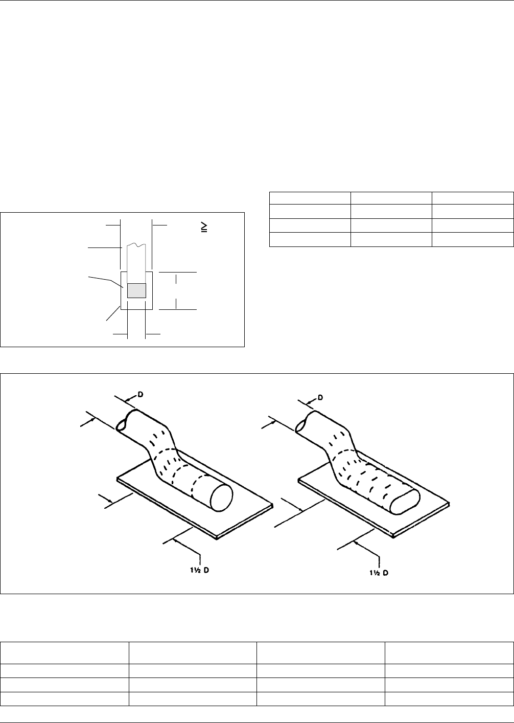
Figure 5–24 Land to ribbon lead relationships
W
Flat Pack Lead
Min. Contact Area
Flat Pack
Land
W
▼
▼
▼
▼
▼
▼
▼
▼
LEAD
LAND
W
L = 2 X W
▼
LEAD
W X W
LEAD
IPC-859-5-25
Figure 5–25 Land contact for round or coined lead
Table 5–3 Maximum and Minumum
Wire Lengths mm [mils]
Wire Diameter Maximum Minimum
0.018 [0.7] 2.03 [100] 0.254 [10]
0.025 [1.0] 2.54 [100] 0.254 [10]
0.038 [1.5] 2.54 [100] 0.380 [15]
December 1989 IPC-D-859
51
5.3.3.2 Automatic Bonding All the requirements
ofmanual wire bonding apply to automatic bonding with
the following exceptions:
A. Wedge bonds—Wedge bonds shall be made only to
gold metallization.
B. Substrate reference locations—At least two reference
locations are required on each substrate; one on the
upper left, the other on the lower right, as shown in
Figure 5–30.
C. Bonding land size—The minimum land size should be
0.254 x 0.254 mm [0.010 x 0.010 inch]. The preferred
land size is 0.38 x 0.38 mm [0.015 x 0.015 inch].
D. Jumper wire length—The preferred jumper wire
length 0.25 to 1.52 mm [0.010 to 0.060 inch]. The wire
length may be extended to 2.03 mm [0.080 inch], but
this may require manual wire dressing.
E. Clearance—The minimum clearance between the bond
and the package wall or component should be in accor-
dance with Figure 5–29. The minimum distance
between the bond and the component when the wire is
connecting component to substrate applies only when a
ball bond is made to component (see Figure 5–31).
F. Platform package pin height—The pin height on plat-
form packages should be greater than 0.51 mm [0.020
inch]. A popular value is 1.27 mm [0.050 inch].
5.3.4 Resistors Preferred thick-film resistor configura-
tions are shown in Figure 5–32. A rectangular configura-
tion is normally used unless the sheet resistivity of the ink
exceeds 320 kilohms per square or the aspect ratio of
length to width is greater than 6.5. For example, an aspect
ratio of 30-to-1 can be achieved after trimming with a top-
hat design. The dotted lines on Figure 5–32 illustrate the
number of squares per resistor in a top-hat configuration
that remain after trimming.
The following should be considered in resistor design:
A. Top-hat resistor designs should not be used for resistors
with tolerances of less than 1 percent.
B. Noise can be reduced in thick-film designs by making
the resistors longer or by increasing total resistor area.
C. Top-hat or meander designs should be considered rather
than conventional rectangular designs in designs where
voltage sensitivity is a problem.
D. Matched resistors should be designed for the same ink,
placed as close to each other as possible and in the
same axis.
E. Cost considerations favor the use of fewer inks. Nor-
mally three different inks or less should be used.
F. Resistors should not be printed on the screened dielec-
tric (insulating layers) directly over underlying conduc-
tors. (See Figure 5–33 for various resistor design tech-
niques.)
G. Dielectric should not normally be printed over a thick-
film resistor. Allow 0.76 mm [0.030 inch] window
allowance on each side of resistor.
5.3.4.1 Dimensional Constraints Table 5–4 lists dimen-
sional constraints for thick-film resistor designs and, in
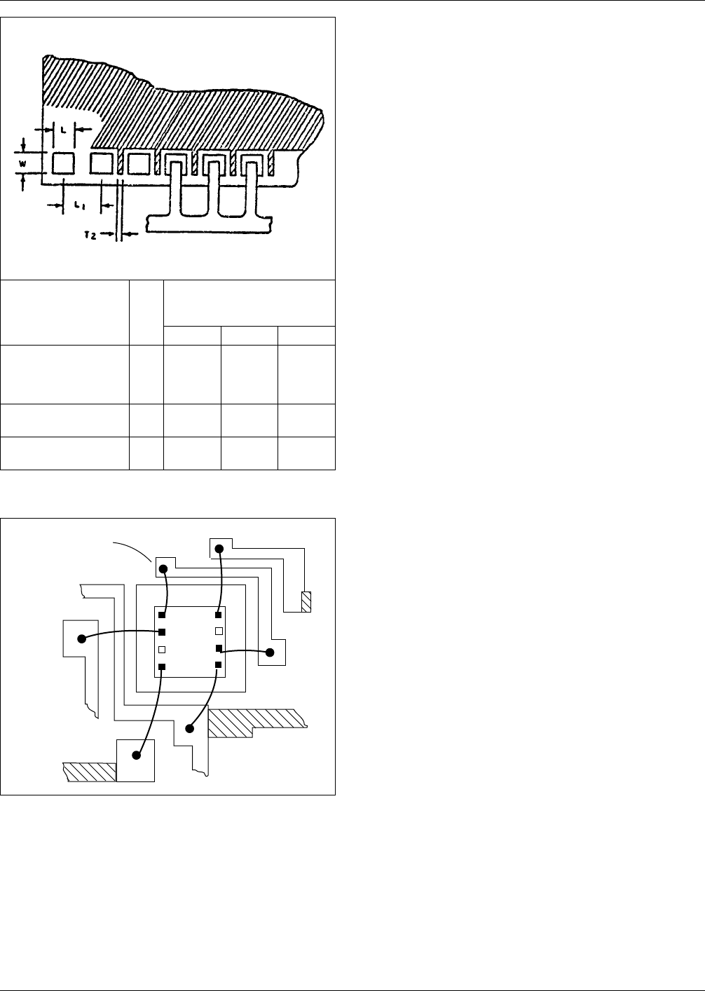
IPC-859-5-26
Dim Producibility mm
[inch]
Most ↔ Least
ABC
Land size, for solder
attachment
L&W 1.52x
[0.060]
1.52
[0.060]
0.76x
[0.030]
1.27
[0.050]
0.76x
[0.030]
1.27
[0.050]
Lead spacing, center
to center
L
1
2.54
[0.100]
1.27
[0.050]
1.27
[0.050]
Screened dielectric
between lands
T
2
0.38
[0.015]
0.25
[0.010]
0.20
[0.008]
Figure 5–26 Minimum lead frame bonding lands, size and
location
IPC-859-5-27
Figure 5-27 Land-to-land IC interconnection
Conductor used for IC land-
to-land connection
▼
1
2
3
4
8
7
6
5
IC
Chip
IPC-D-859 December 1989
52
combination with Figures 5–35 and 5–36 defines recom-
mended values. These dimensions apply equally to rectan-
gular and meander configurations.
5.3.4.2 Resistor Loops Closed resistor loops are not
allowed where trimming must be performed. The proper
method for establishing closed loops is shown in Figure
5–37.
Resistor loops are allowed where the trim system has guard
measurement capability, but this is complex and requires
probing. Shorting bonds may be used to close the loop.
5.3.4.3 Resistor Layout Rules
5.3.4.3.1 Thick-Film Resistor Paste Selection
In some
cases, the selection of pastes may be obvious, especially if
there are only a few resistors or if the values are neatly
clustered. In other instances there may be a large number
of resistors that are widely spread and it may be difficult to
find three or fewer pastes that will cover all resistor values.
A good design avoids the use of more than three resistor
pastes per substrate. The numbers in the left hand column
of Figure 5–38 are standard paste values. The brackets
extending from those pastes show the range of resistor val-
ues that may be screened with each paste. Note that they
overlap.
Figure 5–39 contains generalized design/layout guidelines
for screen printing and locating resistors on a thick-film
substrate.
5.3.4.3.2 Number of Squares After making the selection
of the pastes, the next step in resistor design is to determine
the number of squares that are required to form each resis-
tor value from its assigned paste. The number of squares is
simply the value of the resistor (in ohms) divided by the
value of the paste (in ohms/square):
IPC-859-5-28
Figure 5–28 Wire bonding
Protective
Dielectric
Capacitor
Chip
IC
Chip
Transistor
Chip
Intermediate
Bonding Point
for Chip-to-
Chip Bond
Protective
Dielectric
0.32 x 0.32
[0.0125 x 0.0125]
Bonding Land
Semiconductor
Wire Bonding
Passive Component
Wire Bonding
Exit Land
Wire Bonding Land
Edge of
Substrate
Diode
▼
▼
▼
▼
▼
▼
▼
▼
December 1989 IPC-D-859
53