IPC-D-859.pdf - 第61页
to permit digitizing without dimensioning. Each has mini- mum permitted values. The total resistor area must be large enough to dissipate the specified power . The designer must also be aware of and take into consideratio…
Where: N =
R
ρ
R = Resistance (ohms)
N = Number of squares
ρ = Sheet Resistivity (ohms/square)
The results should be a value between 0.3 and 10. Enter
this value on the worksheet.
5.3.4.3.3 Length, Width, and Power After selecting the
pastes and calculating the number of squares, then the
length and width of the resistor can be determined using
Figure 5–40. Several factors must come together here. The
length and width must each be on grid or must split grids
IPC-859-5-29
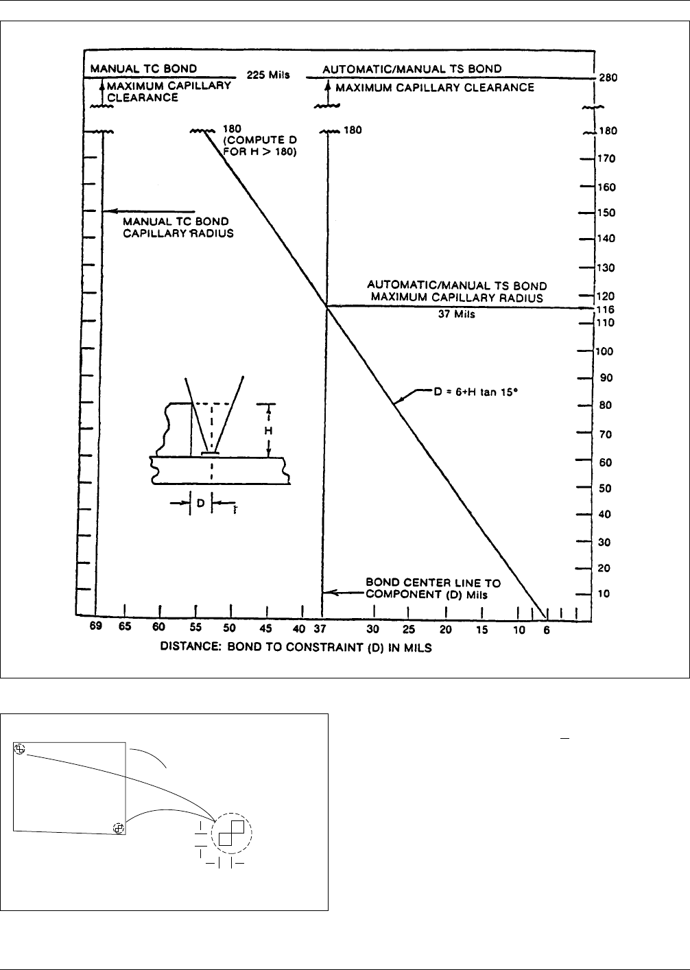
Figure 5–29 Clearances
IPC-859-5-30
Figure 5–30 Autobonding substrate reference locations
▼
▼
D
D
▼
▼
▼
▼
• Reference flag may be rotated 180°
• D = 0.06mm [0.0025"]
• Substrate
▼
IPC-D-859 December 1989
54
to permit digitizing without dimensioning. Each has mini-
mum permitted values. The total resistor area must be large
enough to dissipate the specified power. The designer must
also be aware of and take into consideration variations that
may occur between materials from different suppliers.
The design aid in Figure 5–40 is a simple tool for handling
all of these factors. The left hand column lists resistor
length in half-grid increments. The top row lists widths in
half-grid increments. All other entries in the table are num-
bers of squares:
N =
L
W
Diagonal bands are shown in Figure 5–40. Each of these
bands corresponds to a power dissipation range. The out-
side borders show the power dissipation ranges.
To use these data, simply find a square entry that is close
to the calculated value and which is also within a power
band thatmeets specifications. If there is not a square entry
that is exactly equal to the calculated valued, then select
one that is slightly lower. This will yield a slightly lower
value resistor that can be trimmed to the proper value.
For example, suppose one needs 0.7 squares (a 7-ohm
resistor from 10 ohm/square paste) that must dissipate
160mW. Look in the 150 to 200 mW band. A 0.714 square
resistor might beused. It is 1.27 x 1.78 mm [0.050 x 0.070
inch]. Or a 0.666 square resistor could be used.
The latter would be a better choice for two reasons. First,
0.714 is slightly over the required 0.7 squares. It might be
close enough but it may well yield a resistor that is too
high in value even before trimming. Remember that a resis-
tor can be trimmed only to a higher value. Second, the
0.714 square resistor is right on the 150 mW boundary. It
might be marginal for a 160 mW power dissipation.
In fact, if there is room on the substrate, it would be a good
design practice to use the 0.687 square resistor (1.40 x 2.03
mm [0.055 x 0.080 inch]. This would provide at least a 40
mW safety margin.
5.3.4.3.4 Resistor Design Equations Occasionally there
will be a case where the use of the chart in Figure 5–40 is
not sufficiently precise for the required values. In that case
one will have to calculate the values using equations.
Start by calculating the number of squares and minimum
area required. From these, one will have to calculate the
minimum width and then the minimum length.
The equations are as follows:
(1) A =
P
0.0775 [50]
(2) N =
R
ρ
(3) W =
√
A
N
(4) W = NW
where: A = Minimum area square millimeters
[square inches]
P = Maximum power dissipation (watts)
N = Number of squares
R = Resistor value (ohms)
ρ = Resistor paste value (ohms/square)
W = Width mm [inches]
L = Length mm [inches]
IPC-859-5-31
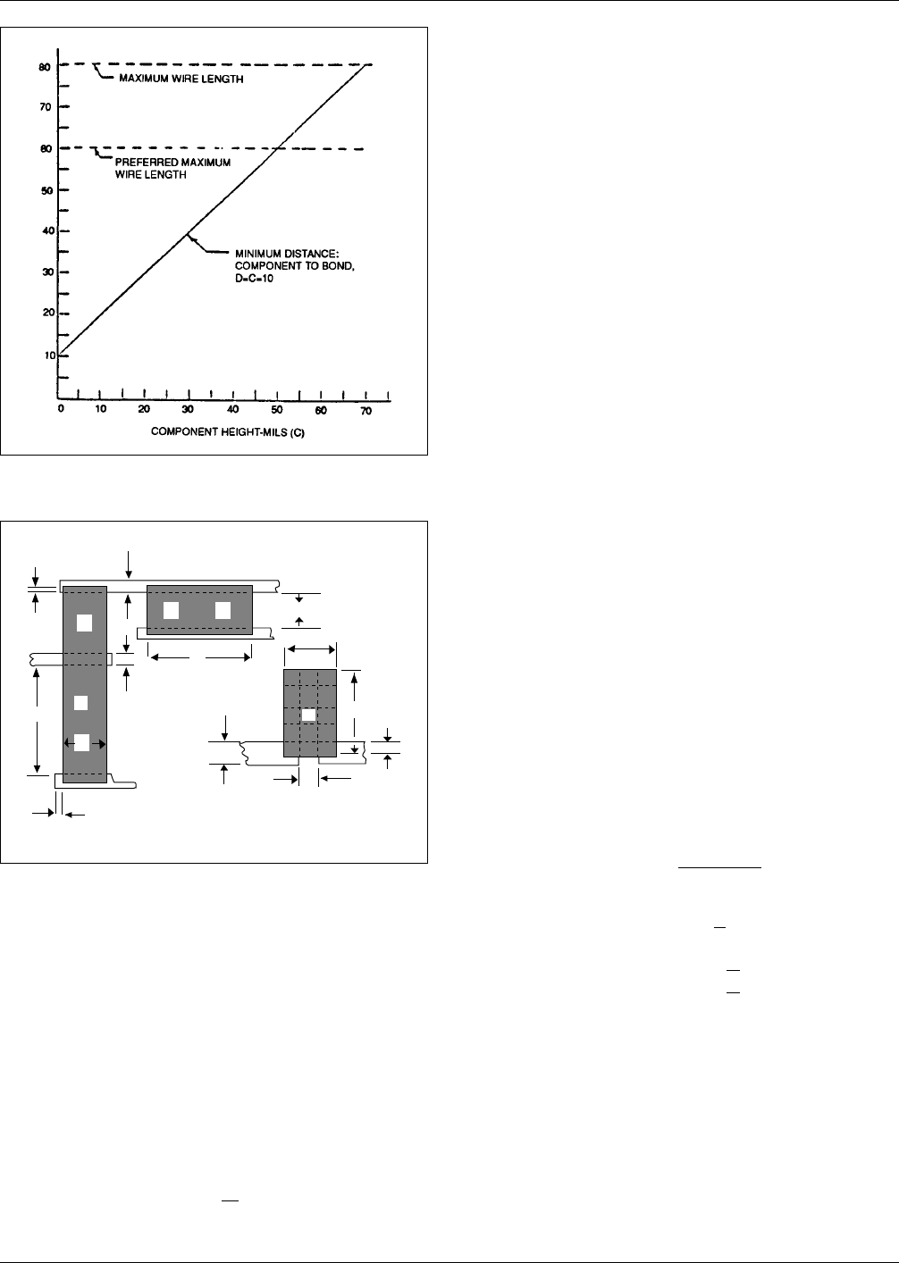
Figure 5–31 Minimum distance between wedge bond and
component as a function of component height.
IPC-859-5-32
Figure 5–32 Preferred thick-film resistor configurations
W
R
R
R
R
W
L
Rectangular
Top Hat
(For Registration Tap)
0.51 [0.020]
0.32 [0.0125]
1.02 [0.040]
0.19 [0.0075]
0.32
[0.0125]
Overlap
Overlap
0.32
[0.0125]
0.51
[0.020]
L
H
L
December 1989 IPC-D-859
55
For example, suppose one must design a 39 Kohm resistor
using 10 Kohm/square paste. It must dissipate 500 mW.
(1) A =
P
0.0775
=
0.500
0.0775
= 6.45 mm
2
A =
P
50
=
0.500
50
= 0.01 m
2
(2) N =
R
ρ
=
39,000
10,000
= 3.9
(3) W =
√
A
N
=
√
6.45
3.9
= 1.29 mm
=
√
[0.01]
3.9
=[0.051 inch]
(4) L = NW = 3.9 x 1.29 = 5.05mm
= 3.9 x [0.051]=[0.199 inch]
The resistor example would have to be dimensioned for
digitizing, would be screened at the exact value (hopefully
not higher) and would run at maximum dissipation. This is
not good design practice. If the design permits, one could
arbitrarily boost the area from 6.45 mm
2
[0.01 inch
2
]to
9.68 mm
2
[0.015 inch
2
] so that the resistor would run
cooler. Then one could recalculate the width and round it
off to the nearest grid or split grid. Finally, it is necessary
to recalculate the length and round it down to the next
lower grid or split grid.
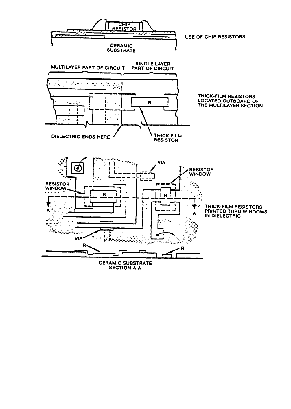
IPC-859-5-33
Figure 5–33 Three methods showing the use of resistors with multilayer thick-film designs (see Figure 5–34 for window
allowance).
IPC-D-859 December 1989
56