IPC-D-859.pdf - 第65页
Magnetic tape may also be supplied for drilling and rout- ing machines. Data tapes supplied in the D–350 series for- mat, shall be single- image, unless otherwise specified. 5.5.1 Artwork Masters A copy of the 1:1 artwork…
A. Via window sizes and spacings should be as shown in
Figure 5–41.
B. The selection of a via design will depend on the spe-
cific layout of the adjacent conductor levels; Figure
5–42 illustrates typical examples. Allow as much over-
lap between the top and bottom conductors as possible
within the design constraints.
C. The vias should be staggered as shown in Figure 5–43,
when routing a conductor from an upper level to the
bottom level. Although this uses more room than does
the routing of a conductor directly through a single
window, yield and reliability are improved. (The print-
ing of a conductor through the thickness of two dielec-
tric layers can result in low yields.)
D. If design or space restrictions prevent the staggering of
vias on adjacent levels, an alternate means of routing a
conductor through multiple levels should be used such
as that is shown in Figure 5–44. With this arrangement
a blind through-hole land is printed through the via
window on the second level to contact the bottom con-
ductor. The top (or third level) conductor is then printed
through another via window to contact the blind land
on the second level.
5.4 Coatings and Markings
5.4.1 Conformal Coatings
The use of conformal coat-
ings shall be in accordance with IPC-CC-830, and may be
any one of the following:
Type AR—Acrylic Resin
Type ER—Epoxy Resin
Type FC—Fluorocarbon Resin
Type SR—Silicon Resin
Type UR—Polyurethane Resin
Type XY—Paraxylene Resin
5.4.2 Compatibility The use of coatings, including the
substrate preparation/cleaning required prior to their appli-
cation, shall be compatible with all other parts and materi-
als used in the hybrid circuit, and the hybrid circuit assem-
bly.
Marking, shown in paragraph 5.4.3, and conformal coating,
shall all be compatible.
5.4.3 Legends When specified on the master drawing,
marking inks may be used to provide identification mark-
ing on the hybrid circuit to provide reference designators,
part numbers, revision status, orientation/polarization sym-
bols, bar codes, etc. Marking inks shall be nonconductive
non-nutrient and shall be able to withstand assembly pro-
cesses. Legends shall be of sufficient size and clarity to
optimize their usage. Usually a minimum height of 1.5 mm
[0.060] with a minimum line width of 0.3 mm [0.012] is
used.
5.5 Artwork Artwork generation and measurement tech-
niques shall be in accordance with requirements of IPC-D-
310.
The appropriate artwork tolerances and allowances shall be
incorporated into the production of the phototool. Single-
image masters, as well as multiple masters may be pro-
vided as part of the data package.
The appropriate media for producing artwork, film or glass,
shall be used. IPC-D-310, indicates the dimensional change
due to changes in temperature and humidity on each of
these products.
When required, the artwork shall have incorporated into it
quality conformance coupons, as stated in paragraph 3.2.
Symbolization artwork to define legend, shall also be sup-
plied as a part of the tooling package (see IPC-D-325).
When computer generated artwork is supplied, it shall be
supplied in magnetic tape format. The IPC artwork shall be
described in IPC-D-350, ‘‘Numerical Control Terms.’’
IPC-859-5-36
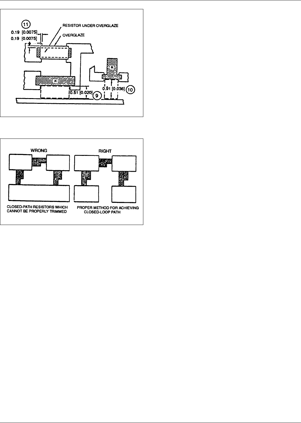
Figure 5–36 Nominal thick-film resistor dimensions for
trimming and overglazing (see Table 5–5)
IPC-859-5-37
Figure 5–37 Closed resistor loops
IPC-D-859 December 1989
58
Magnetic tape may also be supplied for drilling and rout-
ing machines. Data tapes supplied in the D–350 series for-
mat, shall be single- image, unless otherwise specified.
5.5.1 Artwork Masters A copy of the 1:1 artwork mas-
ter for each layer shall be provided as part of the drawing
set. Each artwork master shall contain a minimum of three
(3) dimensioned targets. These targets shall be on grid, and
shall register with each other from layer to layer.
5.5.2 Base Material The artwork master shall be sup-
plied on 200 µm [0.0075 ± 0.005 inch] thick biaxially ori-
ented, dimensionally stable, polyester type film, or on glass
photographic plates.
5.5.3 Accuracy The accuracy of the artwork master shall
be such that each artwork master shall have all centers of
land areas, conductors, and other features located with
respect to the true grid position within the positional toler-
ances established. For the composite artwork master, the
features of all layers shall coincide within the tolerance
specified.
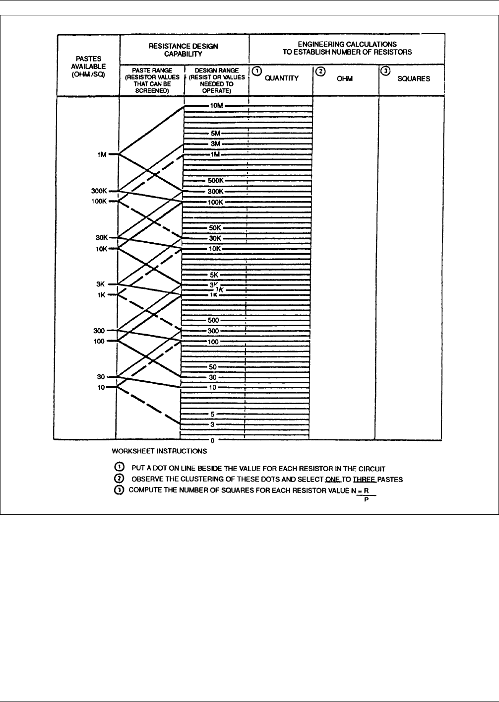
IPC-859-5-38
Figure 5–38 Worksheet for determining resistor pastes based on number of squares needed.
December 1989 IPC-D-859
59
5.5.4 Pinholes There shall be no pinholes on the 1:1 art-
work master larger than 25 µm [0.001 inch], or which
reduce the artwork conductor width by more than 10 per-
cent. Areas outside of the functional board outline shall not
be subject to inspection, and may have pinholes. Pinholes
within the functional board outline that are covered with
opaque ink shall be acceptable.
5.5.5 Opaque Defects (Specks) There shall be no
opaque defects within the functional board outline larger
than 25 µm [0.001 inch] on the 1:1 artwork master, or
which reduce the conductor width by more than 10 percent.
Areas outside of the functional board outline shall not be
subject to inspection, and may have opaque defects. Areas
where opaque defects within the functional board outline,
that have been removed with a sharp pointed hand tool,
shall be acceptable.
5.5.6 Reproduction Conditions The temperature, rela-
tive humidity, date, and photographic facility identification
shall appear on each artwork master film in such a manner
that the artwork master can be readily separated from any
photographic reproductions. Alternately, traceability to
records from automatic monitoring and recording facilities
can be specified.
5.5.7 Packaging and Handling of Artwork Masters
Each artwork master 360 mm x 450 mm [14 x 17 inches]
or under, shall be separately packaged in a glass lined or
polyethylene envelope. Artwork master 360 mm x 450 mm
[14 x 17 inches] to 450 mm x 560 mm [14 x 17 inches]
shall be packaged flat in a box, and constrained with a
sheet of low density foam. Artwork master larger than 450
mm x 560 mm [14 x 17 inches] may be rolled (minimum
diameter 76 mm [3 inches]) and enclosed in a container
made of fiberboard or metal. One inch rubberized hair felt
or equivalent shall be placed in each end of the container
for protection.
5.6 Documentation The documentation package for a
printed wiring board should include the master drawing
and copies of the secondary artwork masters. More than
one copy of the master drawing should be supplied to the
vendor. Other documentation, which may be included with
package, could include mag tapes for the generation of
photoplotted artwork and NC tapes for component place-
ment. Documentation shall meet the requirements of IPC-
D-325.
Numerical control tapes should be included with the ven-
dor documentation package when available. These can be
in a paper tape format, or on mag tape, depending on the
vendor’s capabilities. The code in which the tapes are writ-
ten should also be provided.
5.6.1 Master Drawing The master drawing shall meet
the requirements of paragraph 3.3 and IPC-D-325 and
include, as a minimum, the information detailed in Table
5–5.
5.6.1.2 Marking The master drawing shall include the
specification requirement for all supplemental marking,
that is, those markings other than those etched in the pat-
tern. The drawing note shall include the kind of ink or
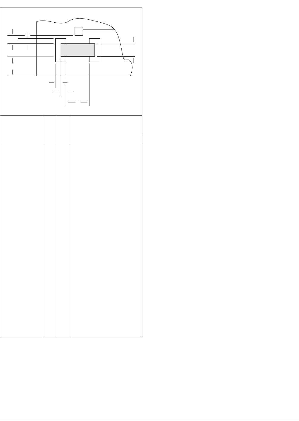
IPC-859-5-39
Dim
Min/
Max
Producibility mm
[inch]
Most ↔ Least
ABC
Screened resistor
size:
• Number of
squares
L/W
L/W
Min
Max
0.5 sq.
5.0 sq.
0.5 sq.
10.0 sq.
0.3 sq.
10.0 sq.
• Length L Min 1.27
[0.050]
1.02
[0.040]
1.02
[0.040]
• Width, ±1% tol-
erance
W Min 1.02
[0.040]
0.89
[0.035]
0.89
[0.035]
• Width, 5% toler-
ance
W Min 0.76
[0.030]
0.64
[0.025]
0.64
[0.025]
Conductor termi-
nal, distance
beyond width
of resistor
D
1
Min 0.38
[0.015]
0.25
[0.010]
0.20
[0.008]
Conductor termi-
nal, distance
beyond length
of resistor
D
2
Min 0.38
[0.015]
0.25
[0.010]
0.20
[0.008]
Resistor overlap,
onto conductor
terminal
D
3
Min 0.25
[0.010]
0.20
[0.008]
0.20
[0.008]
Conductors,
distance from
resistor
D
4
Min 0.51
[0.020]
0.38
[0.015]
0.38
[0.015]
Edge of sub-
strate, distance
from resistor
D
5
Min 0.76
[0.030]
0.51
[0.020]
0.51
[0.020]
Figure 5–39 Thick-film screened resistor sizes
and locations
▼
▼
W
L
D
D
3
2
D
5
D
4
D
1
▼
▼
▼
▼
▼
▼
▼
▼
▼
▼
▼
▼
Screened
Resistor
IPC-D-859 December 1989
60