IPC-D-859.pdf - 第22页
The following are important heat transfer considerations. 3.5.1 Material Selection Select materials with good thermal conductivity . T able 3–3 is a useful guide for mate- rial selection. 3.5.2 Substrate Dimensions Use a…
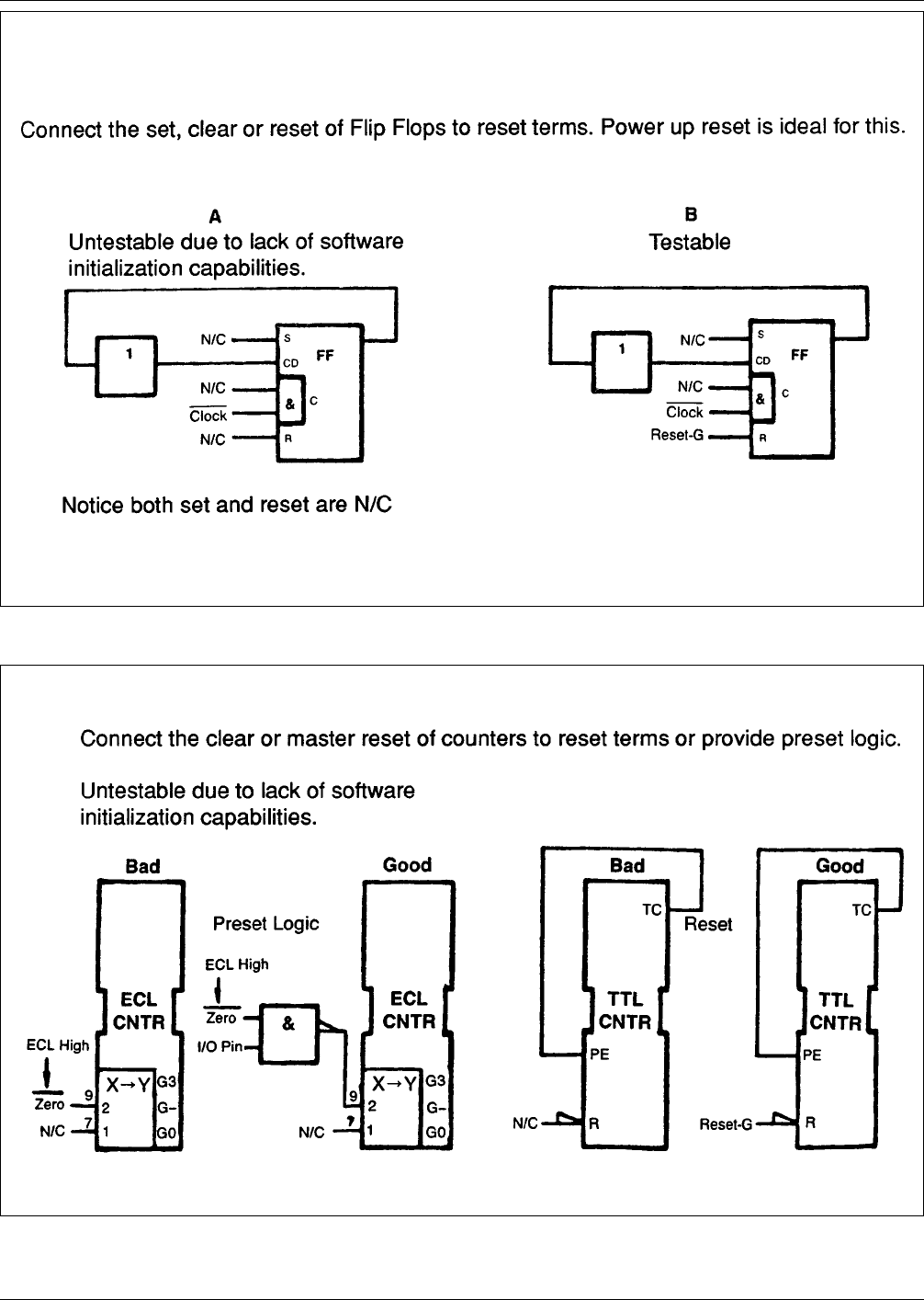
IPC-859-3-11
Figure 3–11 Flip-flop testability
IPC-859-3-12
Figure 3–12 Master clear for counters
December 1989 IPC-D-859
15

The following are important heat transfer considerations.
3.5.1 Material Selection Select materials with good
thermal conductivity. Table 3–3 is a useful guide for mate-
rial selection.
3.5.2 Substrate Dimensions Use a thick substrate for
best heat transfer and distribution unless it is to be bonded
to a heat sink, in which case the thinnest possible substrate
should be used.
The substrate area required for a given electronic circuit is
greatly dependent upon power levels of components. Thus,
low power level circuitry can be packaged more densely
than power circuits.
The use of some first approximation ‘‘rules-of-thumb’’ for
the number of devices (chips) that can be accommodated
with a given technology in various package sizes, would
provide a starting point, together with the thermal consid-
erations, for deciding if the given circuitry needs to be par-
titioned. Another deciding factor in partitioning is the
input/output (I/O) requirements of the circuitry.
3.5.3 General Guidelines
A. Distribute power sources as evenly as possible over the
substrate surface to reduce hot spots and to maintain a
uniform thermal profile.
B. Locate the highest-power sources over or near heat
sinks.
C. Do not locate high-power sources near substrate cor-
ners or edges unless heat sinking is provided in that
vicinity.
D. Design power resistors as large as possible and assure
that sufficient area will be maintained after adjustment.
E. High-heat dissipating components should be attached to
the substrate in such a manner as to provide the lowest
possible thermal resistance between the components
and the substrate.
F. Components should not be attached over the other heat
dissipating elements, i.e., chip capacitors over thick-
film resistors.
G. For best thermal performance, make the junction
between a backside-mounted semiconductor chip and
the substrate with a material of low thermal resistance
that is as thin as possible, and provide a uniform con-
tact area that is free from voids. (In this regard a
knowledge of process capability is critical. If the worst-
case die-attachment wettability is 50%, base heat trans-
fer calculations on the reduced area.)
H. When wire leads or pins are attached to a substrate:
(1) make leads or pins as short as possible, (2) select a
pin material of high thermal conductivity and a pin size
with the maximum possible cross-sectional area,
(3) use as many leads as possible, and (4) locate heat
sources as near to the pins as possible.
I. In final packaging: (1) select a package configuration
that will provide the best thermal conductivity for a
specific application, (2) provide a good thermal con-
duction path between the substrate and the package
case, and (3) avoid air spaces in the thermal conductiv-
ity path if possible. Plastics with high thermal conduc-
tivity can be used to fill voids and improve heat trans-
fer.
3.5.4 Heat Dissipation Calculations The rise in tem-
perature of each component can be estimated using a
model of thermal resistance and power dissipation in which
the temperature rise is calculated as:
T=RxP
where T = temperature rise of the device
above the hybrid case (°C)
R = total thermal resistance between the
device
and the hybrid case (°C/W)
P = power dissipated in the device (W)
The total thermal resistance is calculated by summing the
thermal resistances of each material in the thermal path
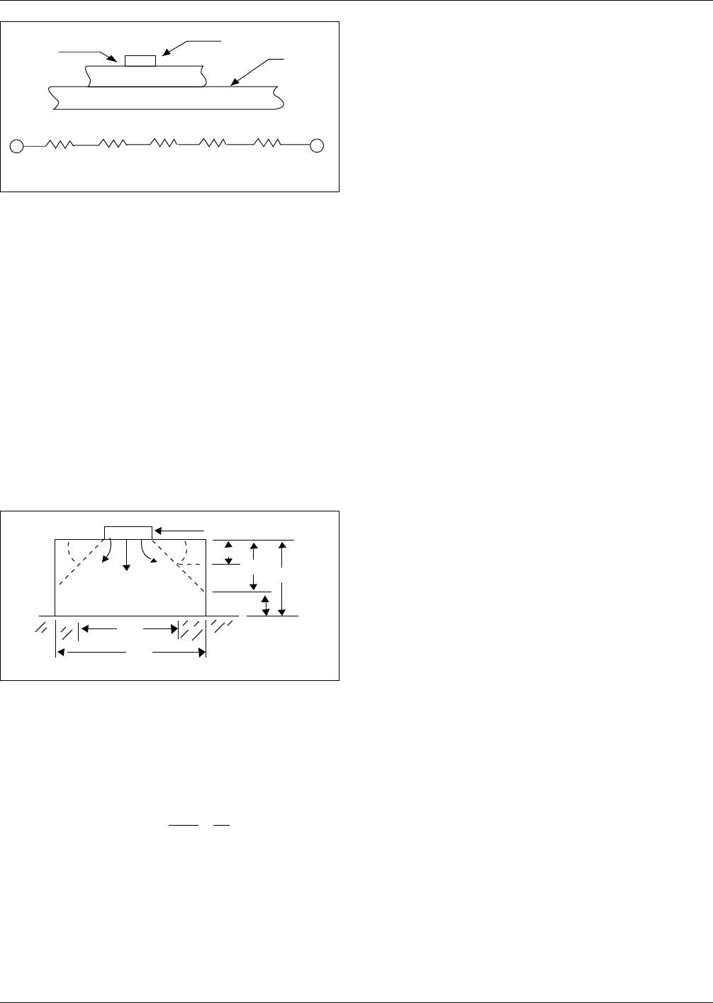
between the device and hybrid case (see Figure 3–13).
Thus:
R
t
=R
1
+R
2
+R
3
+R
4
+R
5
where R
T
= total thermal resistance from the top of the
device to the bottom of the hybrid case.
If parallel thermal paths are involved, the parallel thermal
resistances are totaled in the same manner as are parallel
electrical resistances.
The thermal resistance of a particular material layer is cal-
culated as:
R =
t
KA
Table 3–3 Typical Hybrid Materials Thermal Conductivity
Material
Thermal Conductivity
W/°C/mm
Silicon 58.4
Kovar 9.1
Molybdenum Tab 99.1
Alumina (Al
2
O
3
) 17.5
Beryllia (BeO) 139.7
Conductive Epoxy 1.02
Epoxy Preform 0.25
AuSi Eutectic Bond 144.8
AuSn Solder 114.3
IPC-D-859 December 1989
16
where R = thermal resistance of the material layer
(°C/W)
t = thickness of the material layer (mm)
K = thermal conductivity of the material
in (W/°C–mm)
A = cross-sectional area of the material
layer (mm
2
)
Table 3–3 gives the thermal conductivity of typical materi-
als used in hybrids.
Heat spreading occurs when heat flows into a material
layer of increased cross-sectional area. As illustrated in
Figure 3–14 it is adequate to assume that spreading occurs
at a 45 degree angle.
To calculate thermal resistance when heat spreading
occurs, the average cross-sectional area should be used
over the range of spreading. As shown in Figure 3–13 the
total thermal resistance (R
T
) will be:
R
T
= R
1
=
1/2t
1
KA
1
+
t
2
Ka
Notes: 1. Use average area A over thickness 1/2t
1
. 2. Use area A
over thickness t
2
. 3. No spreading occurs over t
2
.
To the maximum extent possible, devices dissipating sig-
nificant amounts of power should be spaced in the hybrid
in such a manner as to spread the heat flow throughout the
case. When devices are close enough that their areas of
heat spreading overlap, based on the 45 degree assumption,
their thermal interaction should be taken into account. This
can be done by limiting the cross-sectional area used in the
thermal-resistance calculations to areas that do not overlap
the heat spreading of other devices.
When device power dissipation becomes significant, steps
may be taken to minimize the temperature rise. Devices
may be eutectically mounted directly to the substrate or to
ceramic, molybdenum, or kovar ‘‘tabs’’ to increase heat
spreading and to reduce thermal resistance. In extreme
cases, but at considerable cost, devices can be mounted on
Beryllia substrates or metal heat-sinks.
Note that in the above discussion the temperature rise is
related to the hybrid case temperature, not to the ambient
air or to the hybrid mounting surface. The hybrid case tem-
perature will in turn be a function of the ambient air and
mounting surface temperature, the thermal properties of the
mounting surface, and the hybrid to mounting surface inter-
face.
3.5.5 Thermal Matching A primary thermal concern
with ceramic surface-mounted components is the thermal
expansion mismatch between the component and the sub-
strate. This mismatch may result in fractured solder joint
interconnections if the assembly is subjected to thermal
shock, thermal cycling, power cycling and high operating
temperatures. The number of fatigue cycles before solder
joint failure is dependent on, but not limited to, the thermal
expansion mismatch between the component and the sub-
strate, the delta temperature excursion over which the
assembly must operate, the solder joint size, the size of the
component, and the power cycling that may cause an unde-
sirable thermal expansion mismatch if a significant tem-
perature different exists between the component and the
substrate.
With surface-mount components, the number of fatigue
cycles can be increased by reducing the thermal expansion
mismatch, reducing the temperature gradient, increasing
the height of the solder joint, using the smallest physical
size component wherever possible, and by optimizing the
thermal path between the component and the substrate.
3.6 Mechanical Requirement Considerations
3.6.1 Camber
All multilayer hybrids will warp to some
degree unless rigidly supported along all edges. The con-
struction of the board should be as symmetrical as possible
with respect to conductor area distribution and to a lesser
degree, the amount of dielectric applied in which there
exists a Coefficient of Thermal Expansion (CTE) mismatch
between the dielectric and the supporting substrate. Warp-
ing is more likely to occur on the boards having large
width-to-length ratios and in boards having large conductor
areas on one side.
3.6.2 Support All hybrid circuit assemblies should be
supported in order to minimize stress on the components
IPC-859-3-13
Figure 3–13 Example of total thermal resistance
calculation
Mounting
Material
Electrical Device
Substrate
Hybrid
Case
Mounting
Material
Mounting
Material
Electrical
Device
Mounting
Material
Substrate
Hybrid Case
R
R
RRR
5
4
3
2
1
IPC-859-3-14
Figure 3–14 Thermal resistance during heat spreading
ELECTRICAL DEVICE
Heat
45°
45°
A
A
1
t
t
1
1/2 t
1
t
2
December 1989 IPC-D-859
17