IPC-D-859.pdf - 第39页
for optimized testing. This grid should be compatible with assembly and testing equipment, so as to minimize the amount of specialized and complex equipment. For designs where fan-out patterns are not on 0.100 inch grids…

4.1.12.1 Size The size of the hybrid circuits to be auto-
matically assembled can vary substantially. Therefore,
manufacturer’s equipment specifications should be evalu-
ated with respect to the user’s requirements.
4.1.12.2 Surface Mounting Automatic assembly consid-
erations for surface mounted components include pick and
place machines used to assemble chip components, discrete
chip carriers, small outline packages, and flat packs.
Design restrictions shall maintain appropriate clearances
for the automatic pick and place equipment to position the
parts in their proper orientation, and allow sufficient clear-
ances for the placement heads. (See IPC-SM-780.)
Special orientation symbols shall be incorporated into the
design to allow for ease of inspection of the assembled
surface mounted part. Techniques may include special sym-
bols, or special land configurations to identify such charac-
teristics as a pin of an integrated circuit package.
4.1.12.3 Mixed Assemblies Automatic assemblies that
are assembled in two stages require special design consid-
erations in order that the components assembled on the first
phase of the assembly do not interfere with placement
heads during the second phase. Component placement shall
consider the stresses that are put on the substrate by place-
ment equipment, by isolating parts wherever possible, to
specific areas so that the second phase placement stresses
do not impact previously soldered connections.
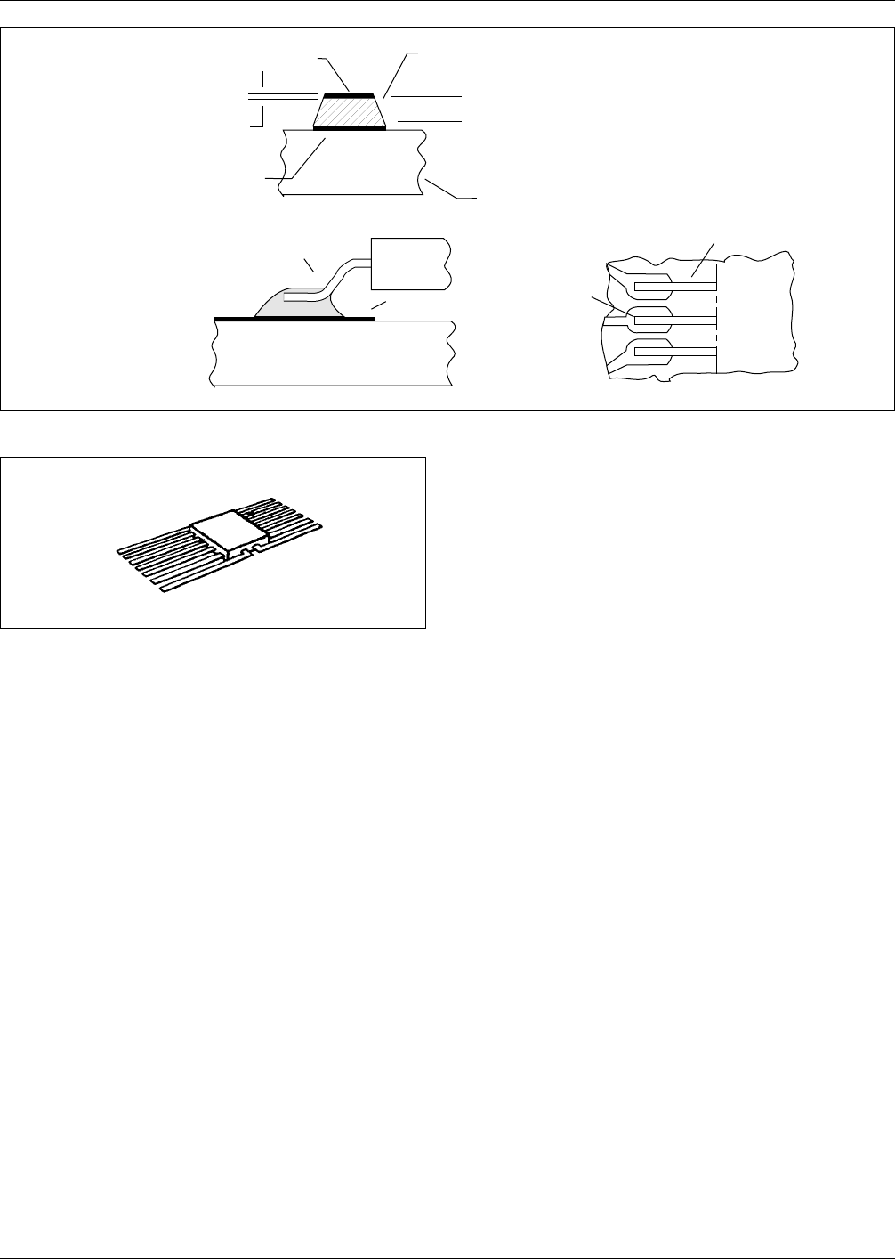
4.2 Surface-Mounted Leaded Components The
requirements and consideration of 4.1.11 apply to the
surface-mounting of leaded components. Lead forming is a
major design consideration and shall be detailed on the
assembly drawing to provide for lead stress relief, fit to the
land pattern, under-body clearance for cleaning, and any
designed-in provisions fro thermal transfer. (See Figure
4–2)
4.2.1 Gull Wing (Flat-Pack) Components Gull wing
components normally have flat ribbon leads that exit from
the component body on 1.27 mm [0.050 inch] lead centers
(Figure 4–3). Although they generally have from 14 to 16
leads, flat-packs with other lead counts are available, some
also with other spacing.
4.2.2 SO I/C’s Small outline (SO) packages are post-
molded plastic packages with lead spacing on 1.25 mm
[0.050 inch] pitch. They are designed to be surface
mounted, and have leads formed outward in gull-wing con-
figurations.
Small outline I/C packages can have 8, 14, 16, 20, 24, 28
leads, and fall into two groups. The leads are two rows of
leads with adjacent leads spaced 1.25 mm [0.050 inch]
apart (see Figure 4–4).
Three-leaded components are used for diodes and transis-
tors. An example of the land pattern outline and package of
the three-leaded package is shown in Figure 4–5.
4.2.3 Plastic Chip Carrier Plastic-leaded chip carriers,
are available as part of the JEDEC package families desig-
nated MS-006, and MS-007. They have leads formed along
the side and under the package body, allowing for either
socket insertion, or direct solder attachment. A representa-
tive lead configuration is a (J) lead, with the (J) going
under the package. Figure 4–6 shows the land pattern mis-
alignment criteria, that should be considered in designing
the land pattern for mounting plastic chip carriers. (See
IPC-SM-782).
4.2.4 Ribbon Lead Termination Flat-wire ribbon leads
may be attached to lands on the hybrid circuit. Connections
shall be made by soldering only.
4.2.5 Round Lead Termination In some instances, com-
ponents with round leads may be attached to the soldered
surface land areas without first passing through a hole. The
land shall be designed with the proper shape and spacing to
comply with proper soldering techniques. Prior to surface
mounting components with round leads, assembly draw-
ings should call for the leads to be formed and coined, to
provide a flat surface of the lead for attachment to the land
area (see Figure 4–7).
4.3 Surface Mount Leadless Components
4.3.1 Chip Carriers
JEDEC Publication 95 presently
covers two chip carrier package styles: 1.27 mm [0.050
inch] (Figures 4–8 and 4–9) and 1 mm [0.040 inch] termi-
nal center-line spacing.
4.3.1.1 Application Considerations General consider-
ations for the application of chip carriers is shown in Table
4–1. For a more detailed analysis see IPC-SM-780 and
IPC-SM-782.
4.3.1.2 Land Patterns The land patterns used with chip
carriers fall into two main categories based on the local
routing density associated with the surface-mounted
device. The selection, design, and position of the land
geometry in relation to the chip carrier have a significant
impact on the desired solder joint configuration. See IPC-
SM-782.
4.3.1.3 Fan-Out The design of fan-out to interconnect
the basic land pattern to other circuitry/devices on a P/I
structure is dependent on wiring density, testability, assem-
bly, repairability and routability requirements.
4.3.1.4 Testing (General) It is recommended that chip
carrier sites be located on a fixed grid within a P/I structure
IPC-D-859 December 1989
32
for optimized testing. This grid should be compatible with
assembly and testing equipment, so as to minimize the
amount of specialized and complex equipment.
For designs where fan-out patterns are not on 0.100 inch
grids (see Figure 4–10, a specialized fixture would be
required for electrical testing.
4.3.1.5 Primary-Side Testing Testing on the primary
side is only recommended for unpopulated P/I structures.
Thus, designing a chip carrier site for primary side testing
does not required dedicated through vias, and thus permits
more efficient routing. This is usually only used with
designs using blind or buried vias, or where the secondary
side is inaccessible. Testing on a 2.54 mm [0.100 inch] grid
is suitable on an ‘‘IL’’ modified fan-out pattern. (See Fig-
ure 4–11)
Testing on an ‘‘II’’ pattern (Figure 4–11) is possible, but
would require dedicated test fixtures with customized 1.27
mm [0.050 inch] pitch probes.
4.3.1.6 Secondary-Side Testing Testing on the second-
ary side is suitable for both populated and unpopulated P/I
structures. In both cases, it should be recognized that nets
ending on non-via lands on the primary side of the P/I
structure will require a via for continuity testing. Thus,
testing on the secondary side requires an ‘‘IL’’ or modified
fan-out patterns with vias and test lands on 2.54 mm [0.100
inch] grid on the secondary side, and corresponding rout-
ing penalty. An ‘‘II’’ land pattern and its associated vias,
not on a 2.54 mm [0.100 inch] grid, would again require a
dedicated test fixture as described for primary side testing.
4.3.2 Leadless Discrete Components (Figure 4–12)
Microminiature leadless devices are available to the circuit
designer in resistor, capacitor, transistor, and zener diode,
chip form. The chips are placed in a nonconductive carrier
and encapsulated in epoxy, or hermetically sealed. All met-
allized surfaces are plated to permit thermo-compression or
ultrasonic bonding.
4.3.2.1 End-Capped Discrete Components End-capped
discrete resistor and capacitor components, and similar
leadless end-capped discrete components, shall not be
stacked, nor shall they bridge spacing between other parts
or components, such as terminals or other properly-
mounted components (see Figure 4–13.)
End-cap discrete leadless components with electrical ele-
ments deposited on an external surface, such as chip resis-
tors, shall be mounted with that surface facing away from
the printed board (see Figure 4–14).
4.3.3 MELF Component metal electrical face leadless
devices are also available in circular fashion. These cylin-
drical devices have the land-to-lead configuration require-
ments shown in Figure 4–15. The same rules for proper
mounting, as discussed in section 4.3.2, apply.
IPC-859-4-2
Figure 4–2 Flat-pack surface mounting
▼
Tinned Lead
▼
▼
Reflowed
Solder
Flat Pack Lead
▼
▼
Land
Flat Pack Lead
Land
Solder
Laminate
3T Maximum
Lead Thickness (T)
▼
▼
▼
▼
▼
▼
▼
IPC-859-4-3
Figure 4–3 Flat-pack multiple-lead component
December 1989 IPC-D-859
33
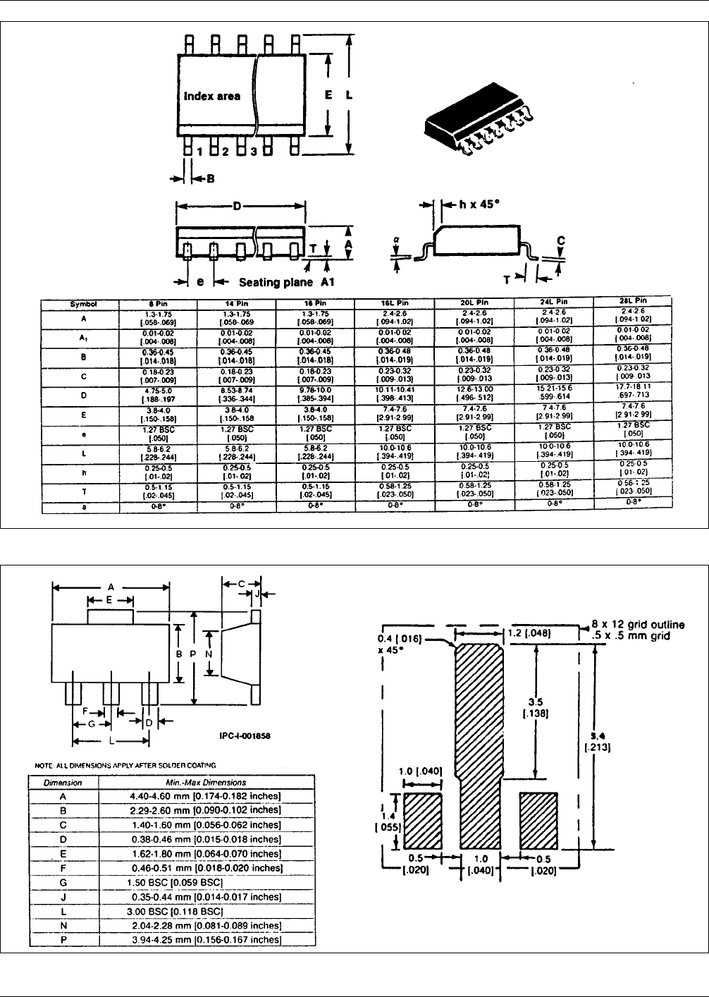
IPC-859-4-4
Figure 4–4 SO 16 integrated circuit package
IPC-859-4-5
Figure 4–5 SOT-89 package drawing example
IPC-D-859 December 1989
34