IPC-D-859.pdf - 第56页
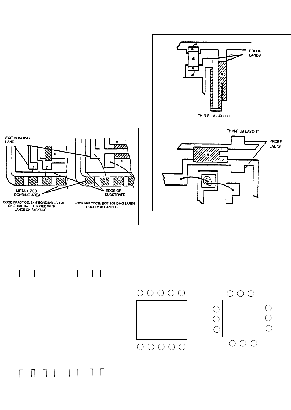
IPC-859-5-21 Figure 5–21 Land pattern leadless chip carrier IPC-859-5-20 Figure 5–20 MELF chip resistors land relationships IPC-859-5-22 Figure 5–22 Fan-out patterns IPC-859-5-23 Figure 5–23 Land to heel/toe configuration…
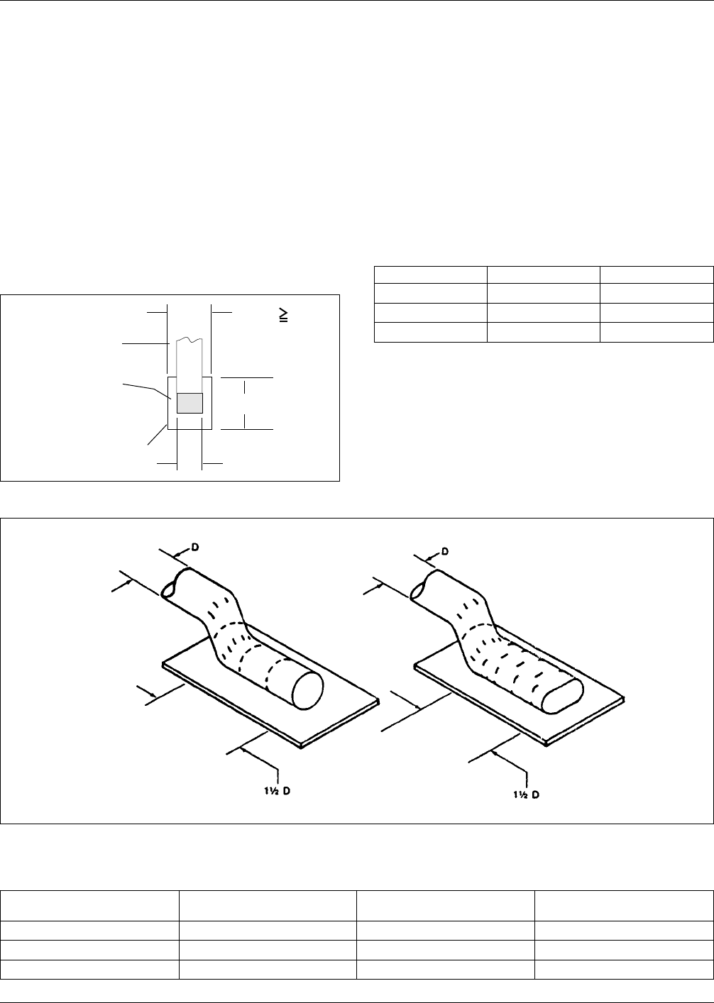
round leads shall have a land which will provide the seat-
ing so that the heel and the terminal relationship is in
accordance with Figure 5–25. Leads shall be seated with no
side overhang. Toe overhang is acceptable, provided that
the flattened lead in contact with the terminal area is a
minimum of 150% of the unflattened lead diameter, and the
overhang does not reduce the spacing to adjacent parts to
less than that specified on the assembly drawing.
5.3.2.10 Lead Frame Bonding Lands Figure 5–26 estab-
lished minimum values for size and location of lead frame
bonding lands.
5.3.3 Wire Bonds Wire-bond connection should never be
made between lands on IC chips. A method for making
such connections is illustrated in Figure 5–27
Wires should never cross other wires or chip components.
When wire bonds cross electrically uncommon conductor
IPC-859-5-17
Figure 5–17 Exit land/alignment/misalignment
considerations for hybrid packages
IPC-859-5-18
Figure 5–18 Examples of lead/pin identification assignments
19 X 19 [0.75" X 0.75"] SUBSTRATE
OUTLINE FOR 16 LEAD
25 X 25 [1" X !"] HAC PAC
PACKAGE
8.76 X 11.2 [0.345 X 0.445]
SUBSTRATE
OUTLINE FOR
10 PIN
12.7 X 12.7 [0.5 X 0.5]
PLATFORM
PACKAGE
8.4 X 8.4 [0.33 X 0.33]
SUBSTRATE
OUTLINE FOR
15.24 [0.0600]
DIA. TO 20.32 [0.800]
PACKAGE
16 15 14 13 12 11 10 9
1 2 3 4 5 6 7 8
10 9 8 7 6 9 8 7
1 2 3 4 5
10
11
12
6
5
4
1 2 3
DIMENSIONS IN mm [INCHES]
IPC-859-5-19
Figure 5–19 Probe land positioning to assist resistor
trimming.
December 1989 IPC-D-859
49
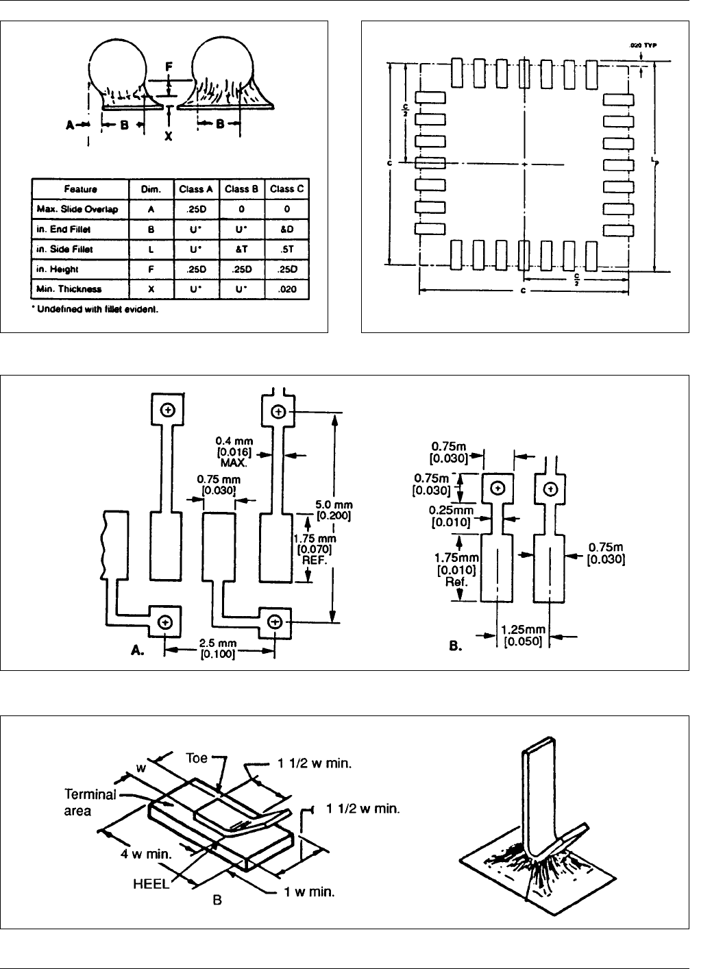
IPC-859-5-21
Figure 5–21 Land pattern leadless chip carrier
IPC-859-5-20
Figure 5–20 MELF chip resistors land relationships
IPC-859-5-22
Figure 5–22 Fan-out patterns
IPC-859-5-23
Figure 5–23 Land to heel/toe configurations
IPC-D-859 December 1989
50
metallizations, the conductor metal shall be covered with-
protective dielectric to prevent sagging wire bonds from
causing catastrophic failure. Figure 5–28 illustrates
examples of this principle.
5.3.3.1 Manual Bonding The following should be con-
sidered if manual wire bonding is utilized.
A. Wire types—Minimum manual-bonding wire size
should be checked to ensure sufficient current-carrying
capacity. See Table 5–2.
Due to the small (0.076 to 0.127 mm [0.003 to 0.005
inch]) size of the bonding lands on transistors and
diode chips 0.178 mm [0.007 inch] diameter, wires can
be used for manual wire bonding of these devices, how-
ever, the designer should provide the largest possible
mounting and bonding lands on the substrate. This not
only facilitates initial bonding, but provides room for
the making of additional bonds should the device need
to be replaced or repaired. Use of 0.025 mm [0.001
inch] diameter wire is preferred.
B. Wire bond parallelism—Wire bonds should parallel
the substrate edge if possible.
C. Wire length—Maximum and minimum wire length
between bonds should be as shown in Table 5–3.
D. Adjacent wire location—No wire should cross another
wire. Therefore, the layout should provide for the maxi-
mum separation allowed by the device geometry.
E. Clearance—The minimum bond-to-package wall or
component clearance is shown in Figure 5–29.
Table 5–2 Current Ratings and Resistance for Gold Wire
Wire Size
mm [mils]
Rated Current
(mA)
Glow/Failure Current
(mA)
Resistance
ohms/mm [inch]
0.018 [0.7] 160 350 0.094 [2.38]
0.025 [1.0] 250 520 0.046 [1.16]
0.038 [1.5] 400 840 0.020 [0.518]
IPC-859-5-24
Figure 5–24 Land to ribbon lead relationships
W
Flat Pack Lead
Min. Contact Area
Flat Pack
Land
W
▼
▼
▼
▼
▼
▼
▼
▼
LEAD
LAND
W
L = 2 X W
▼
LEAD
W X W
LEAD
IPC-859-5-25
Figure 5–25 Land contact for round or coined lead
Table 5–3 Maximum and Minumum
Wire Lengths mm [mils]
Wire Diameter Maximum Minimum
0.018 [0.7] 2.03 [100] 0.254 [10]
0.025 [1.0] 2.54 [100] 0.254 [10]
0.038 [1.5] 2.54 [100] 0.380 [15]
December 1989 IPC-D-859
51