IPC-D-859.pdf - 第42页
as mismatch of Coef f icients of Thermal Expansion, solderability/weldability of the material, and protection of its contacts from corrosion during storage. When flexible cable is used, it may be soldered directly to land…
4.4 Component Lead Sockets
4.4.1 Integrated Circuit Sockets
4.4.1.1 DIP Sockets
Sockets, such as that shown in Fig-
ure 4–16 are designed for low-cost, high-density, mounting
of DIP components. They are generally designed to resist
solder wicking into the socket or cavity, and have provi-
sions that provide the needed clearance of the socket above
the substrate.
4.4.1.2 Chip Carrier Socket Sockets such as that shown
in Figure 4–17 can be used with most of the chip carriers
described in 4.3.1. They can be either surface mounted or
through-hole mounted, depending on the termination con-
figuration of the socket contacts.
When they are surface mounted, they can also be obtained
with a mechanical contact pressure interface to the printed
board. The advantages of this type of socket are the ease of
replacement of the socket, and the absence of damage due
to soldering and unsoldering. A disadvantage is that a sec-
ond mechanical interface is now in the circuit path.
4.5 Connectors and Interconnects One of the critical
design requirements for multilayer hybrid circuits is to pro-
vide a method of interconnection for signal and power
input/outputs.
This is normally done by surface contact to lands on the
outer layer(s), typically with a conductive header or by the
use of flexible circuitry.
When the header is used, it may be soldered, welded or
brazed to the surface lands, with its contacts projecting
beyond the periphery of the substrate. In selecting material
for the header, consideration should be given to such items
IPC-859-4-6
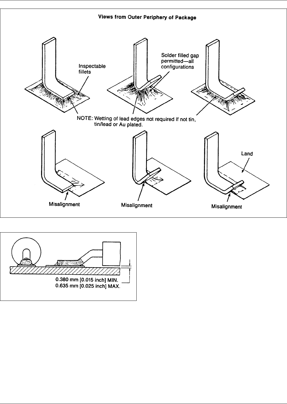
Figure 4–6 Plastic-leaded chip carrier lead misalignment
IPC-859-4-7
Figure 4–7 Round or coined lead
December 1989 IPC-D-859
35
as mismatch of Coefficients of Thermal Expansion,
solderability/weldability of the material, and protection of
its contacts from corrosion during storage.
When flexible cable is used, it may be soldered directly to
land patterns on the substrate. Proper mechanical support,
using tie-down bars, or adhesives, shall be used to prevent
stresses on the solder joints.
IPC-859-4-8
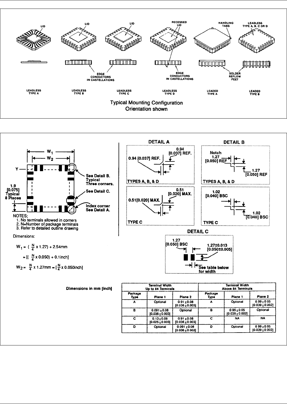
Figure 4–8 JEDEC 1.27 mm [0.050 inch] chip carrier packages
IPC-859-4-9
Figure 4–9 Common features of JEDEC 1.27 mm [0.050 inch] center chip carriers.
IPC-D-859 December 1989
36
In either case, if the assembly is to encounter a great deal
of vibration or shock, additional mechanical support should
be provided.
4.6 Special Wiring
4.6.1 Jumper Wires
It may be necessary to add point-
to-point wiring to a hybrid. Such wiring shall beconsidered
as not being part of the hybrid circuit, but as part of the
assembly process. Therefore, their use shall be documented
on the hybrid circuit master drawing.
4.6.1.1 Types Point-to-point (jumper) wires are usually
of the following types:
A. Bare bus wire that consists of a single strand of wire
that is of sufficient cross-section to be compatible with
the electrical requirements of the circuit without the use
of sleeving or other insulation.
B. Sleeved bus wire that consists of a single-strand of bare
bus wire (see A above) that is covered by insulation
tubing
C. Insulated bus wire that consists of a single strand wire
that has its own insulation when purchased, either a
plastic or varnish coating.
D. Insulated stranded wire that consists of multiple strands
of wire that are purchased with a plastic coating
4.6.1.2 Application The use of jumper wires should
adhere to the following rules:
A. Bare bus wires should not be longer than one inch.
B. Bare bus wires should not cross over hybrid conduc-
tors.
C. Bend radii for jumper wires should conform to that of
normal component bend requirements (see 4.1.11).
D. The shortest path of jumper routing should be used
unless hybrid design considerations dictate otherwise.
E. Sleeving should be of sufficient length to ensure that its
slippage at either end of the jumper wire will not result
in a gap between the insulation and solder joint or wire
bend of more than 3.2 mm [0.125 inch]. Also, the
sleeving should not be damaged by the jumper wire or
hybrid circuit soldering operations.
4.6.2 Bus Bars Bus bars are usually preformed compo-
nents in the hybrid circuit assembly that provide most, if
not all, of the power and ground distribution over the cir-
cuit surface. They are used primarily to minimize power
and ground distribution circuitry or to provide power and
ground distribution not provided by the hybrid circuit.
The number of conductor levels in the bus bar, the type and
number of their terminals, the size and finish of their con-
ductors, and the dielectric strength of the insulation
Table 4–1 Chip Carrier Application Considerations
Consideration Leadless CC’s Leaded CC’s
Thermal expansion to match P/I structure Critical Less critical
Removal and replacement Comparatively easy with special tools.
Less risk of damaging P/I
Solder joint inspection Difficult Less difficult
Flux removal after soldering Difficult Less difficult
Socket compatible Yes (except Type C) Yes (except Type B)
Lead length (CC-land pattern) Minimal Moderate (inductance greater)
Conductive cooling Good, with direct head conduction path
(Lower profile height)
Preparation for soldering Solder coating of terminals required None except for solder coating as required
for solderability
Self centering Usually Rarely
Flexure of P/I structure Critical Less critical
IPC-859-4-10
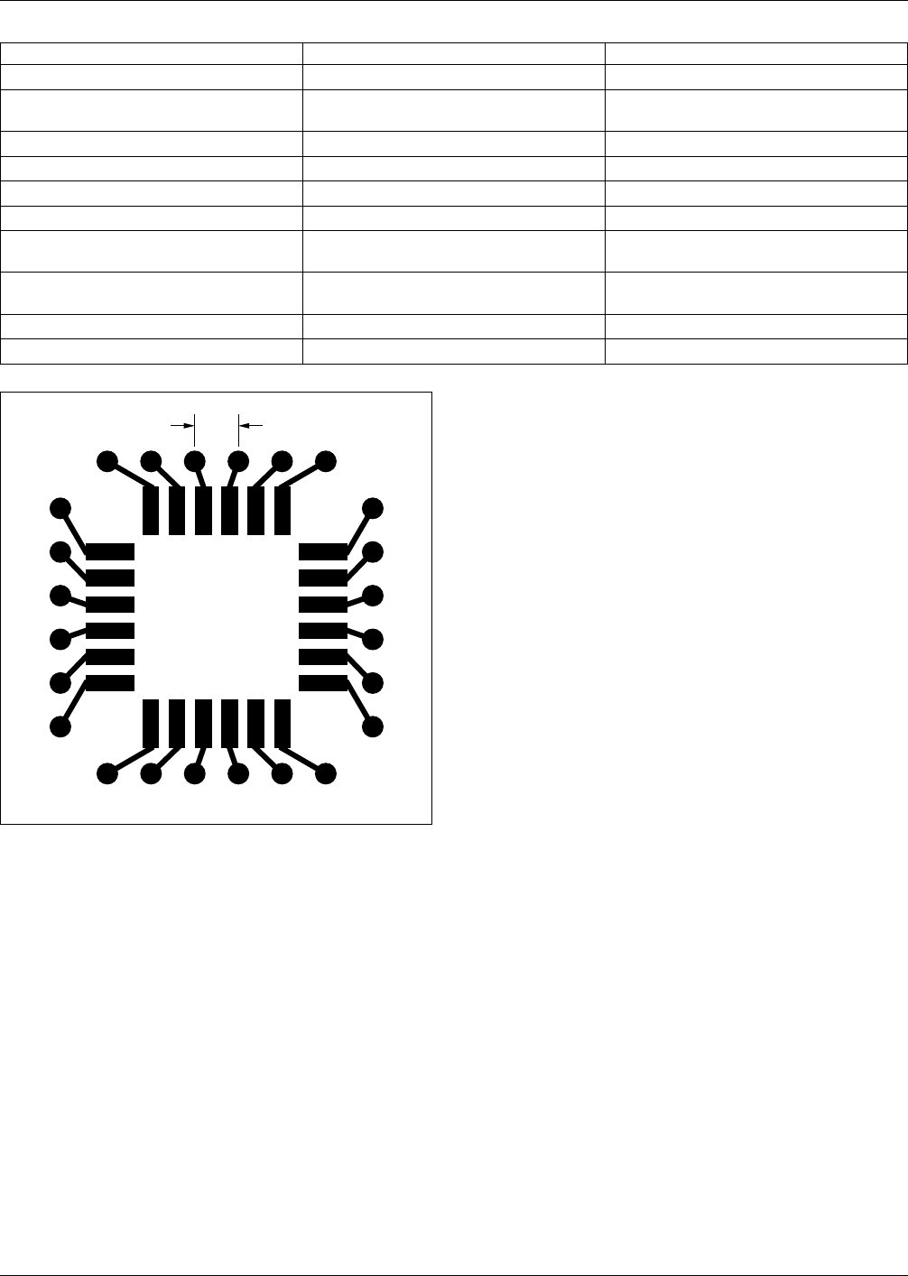
Figure 4–10 24-I/O, 1.02 mm [0.040 inch] pitch, fan-out
pattern on a custom grid
2.0
[0.080]
December 1989 IPC-D-859
37