IPC-D-859.pdf - 第51页
E. The maximum number of conductor levels for high yields is three. Processing yields may be af fected with additional layers, although an infinite number of layers are theoretically possible. F . Semiconductor chips, cap…
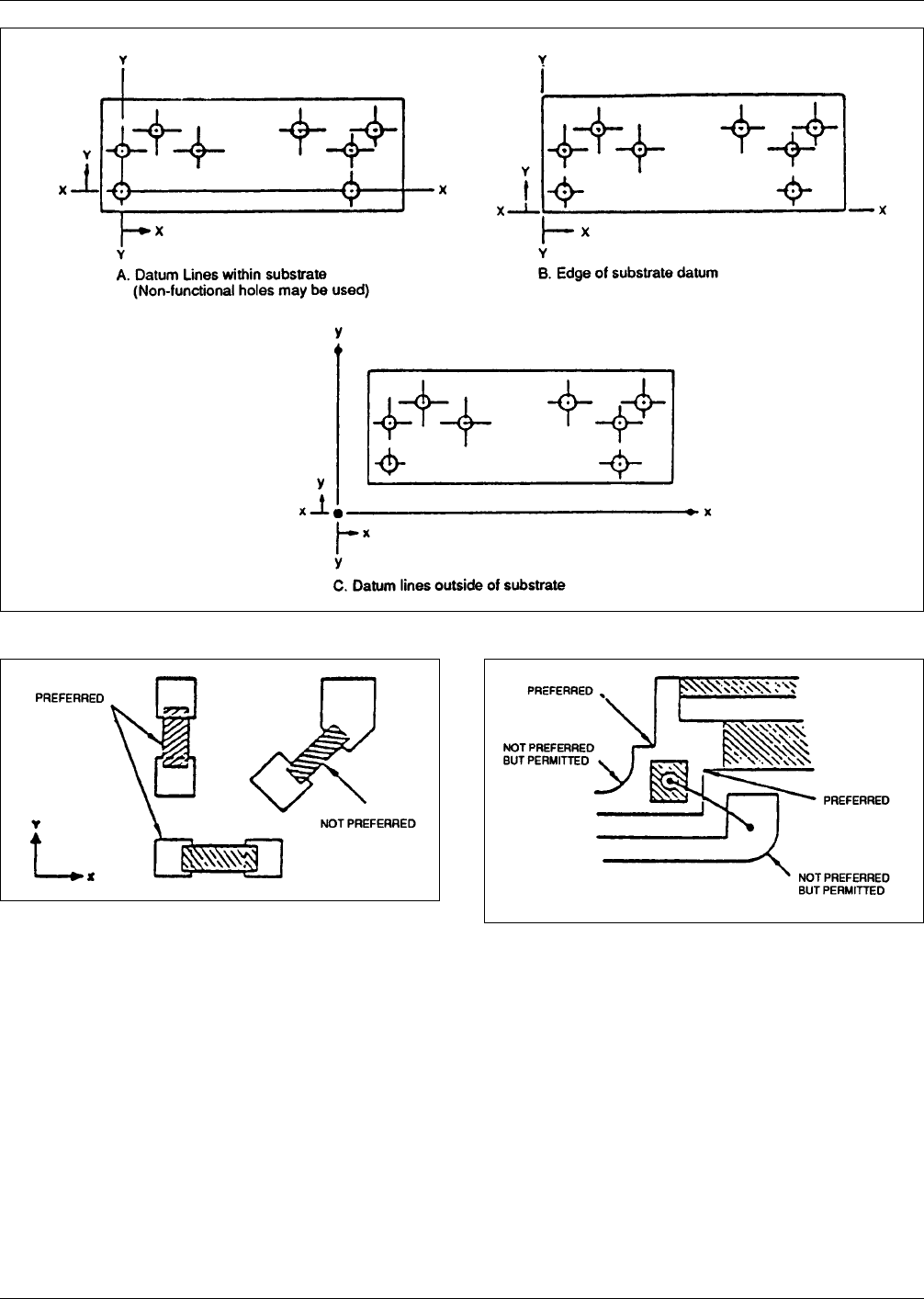
Conductor junctions, the corners of mounting lands and
conductor-resistor patterns should be designed with right-
angled edges and turns as shown in Figure 5–5. Rounded
corners, which can be generated when photoplotters are
used for artwork, are not preferred but are permitted.
5.3.1.3 Conductor Spacing Minimum conductor spac-
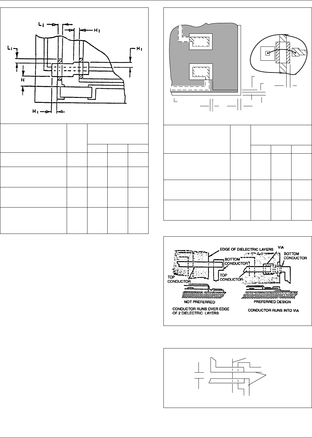
ing shall be in accordance with Table 3–1 and Figures 5–6
and 5–7.
5.3.1.4 Conductor Layout Guidelines The following
guidelines should be observed during the layout of thick-
film multilayer circuits:
A. Avoid running conductors over the edge of multiple
dielectric layers; use vias (see Figure 5–8).
B. The spacing between conductors must be a minimum of
0.38 mm [0.015 inch] if it is necessary to run conduc-
tors over the edge of a single dielectric layer (see Fig-
ure 5–9).
C. Avoid running conductors parallel to other conductors
that are directly beneath them for long distances (see
Figure 5–10).
D. An overlap at least 0.25 mm [0.010 inch] is recom-
mended where a top and bottom conductor connect to
one another (see Figure 5–11).
IPC-859-5-3
Figure 5–3 Establishing datums
IPC-859-5-4
Figure 5–4 Orientation for conductor–resistor patterns
IPC-859-5-5
Figure 5–5 Land and conductor geometries
IPC-D-859 December 1989
44
E. The maximum number of conductor levels for high
yields is three. Processing yields may be affected with
additional layers, although an infinite number of layers
are theoretically possible.
F. Semiconductor chips, capacitor chips, and resistor
chips may be mounted on lands on the top conductor
level of multilayer thick-film designs. Also, ultrasonic
wire bonds may be made from the chips to the lands;
however, it is recommended that thermo-compression
bonds be made only to bottom level conductors. If
thermo-compression bonds must be made to the top
conductor level, a double conductor layer should be
used for the land (see Figure 5–12)
G. Provide test points for short-circuit and continuity
checking between conductor levels.
5.3.2 General Requirements for Lands and Bond Lands
The following general requirements shall be met for all
lands and bond lands.
IPC-859-5-6
Dim
Producibility mm
[inch]
Most ↔ Least
ABC
Resistor
distance to dielectric
H 1.27
[0.050]
1.14
[0.045]
1.14
[0.045]
Conductor lines staggered,
1
distance to dielectric step
(typical on 2-layer circuit).
H
1
0.51
[0.020]
0.38
[0.015]
0.25
[0.010]
Conductor lines overlap
L
1
0.38x
0.38
[0.015]
0.25x
0.25
[0.010]
0.25x
0.25
[0.010]
Dielectric crossover,
distance extended beyond
width (on either top or
bottom conductor).
H
1
0.51
[0.020]
0.38
[0.015]
0.38
[0.015]
1. A staggered dielectric configuration is required whenever two (closely
placed) adjacent conductors are screened over a dielectric crossover.
Figure 5–6 Minimum dielectric distance from other lines
and for crossovers.
IPC-859-5-7
Dim
Producibility mm
[inch]
Most ↔ Least
ABC
Dielectric distance to
metallized land for solder
or epoxy component
attachment.
W 0.38
[0.015]
0.25
[0.010]
0.25
[0.010]
Dielectric distance to edge
of substrate, minimum
sized
W
1
0.25
[0.010]
0.13
[0.005]
0.13
[0.005]
Dielectric width, when
covering conductors that
run under bond wire.
W
2
0.25
[0.010]
0.13
[0.005]
0.13
[0.005]
Figure 5–7 Minimum dielectric spacing and size
▼
▼
▼
▼
▼
▼
▼
▼
▼
Substrate
Edge
W
2
W
1
W
1
W
W
2
Solder
Pad
Solder
Pad
▼
▼
DEVICE
IPC-859-5-8
Figure 5–8 Conductor interconnects external to the
dielectric
IPC-859-5-9
Figure 5–9 Spacing between adjacent conductors
running over a dielectric edge.
▼
0.38mm
[0.015"] min.
Dielectric Edge
Bottom
Conductors
▼
▼
▼
▼
December 1989 IPC-D-859
45
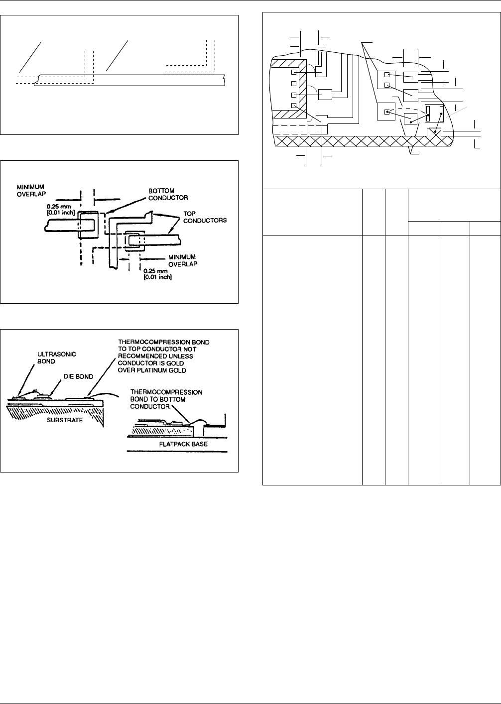
5.3.2.1 Bond Lands Wire bond land sizes shall be in
accordance with Figure 5–13.
Figure 5–14 shows recommended locating dimensions to
provide access and clearance for the bonding tool head.
5.3.2.2 Component Mounting Lands Figure 5–15 estab-
lishes minimum lands for component mounting.
Nominal dimensions and spacing for chip mounting lands
are shown in Table 5–1 and Figure 5–16.
5.3.2.3 Exit Land/Package Lead Alignment Layouts
should be prepared with the exit bonding lands on the sub-
strate in alignment with the metallized bonding areas or
pins of the hybrid package. An example of proper and
improper location of lands is shown in Figure 5–17.
Figure 5–18 illustrates a recommended approach for iden-
tifying exit lead/pins for standard packages.
5.3.2.4 Probe Lands When space allows, probe lands
should be included for trouble-shooting and for use with
resistor trimming. For this latter purpose, lands should be
placed as close as possible to resistor terminations as
shown in Figure 5–19. (Note: The recommended size for
probe lands is 0.51 mm [0.020 inch] square.)
5.3.2.5 Lands ‘‘MELF’’ Discrete Components MELF
discrete components, when mounted as defined in 4.3.3,
shall have their land relationships identified as shown on
Figure 5–20.
IPC-859-5-10
Figure 5–10 Preferred parallel conductor design
Top
Conductor
▼
Bottom
Conductor
▼
One conductor directly over
another
Conductors not over or under
each other
Poor Design Preferred Design
IPC-859-5-11
Figure 5–11 Overlap between top and bottom conductors
IPC-859-5-12
Figure 5–12 Examples of die bonds and wire bonds in
multilayer thick-film designs
IIPC-859-5-13
Dim
Min/
Max
Producibility mm
[inch]
Most ↔ Least
ABC
Wire Bond Land Sizes:
• Length
L Min 0.51
[0.020]
0.38
[0.015]
0.30
[0.012]
• Width, single wire
W Min 0.38
[0.015]
0.25
[0.010]
0.20
[0.008]
• Width, double wire
W
2
Min 0.64
[0.025]
0.51
[0.020]
0.38
[0.015]
Locating angle, die edge to
center of wire bond site.
< Min 90° 45° 45°
Die edge distance to edge
of land:
• Maximum
D
1
Max 1.78
[0.070]
2.54
[0.100]
2.54
[0.100]
• Minimum or 2.5 x thick-
ness of die (whichever
is greater).
D
2
Min 1.27
[0.050]
0.76
[0.030]
0.64
[0.025]
Dielectric distance to center
of wire bond site
D
3
Min 0.5
[0.020]
0.38
[0.015]
0.25
[0.010]
Wrap around metallization
distance to center of wire
bond site.
T Min 0.76
[0.030]
0.64
[0.025]
0.64
[0.025]
Figure 5–13 Wire bond land sizes and locations (wire
bonds shall not be placed on via fill metallization.)
▼
▼
▼
▼
▼
YES
NO
IC
DEVICE
DEVICE
W
W
L
2
D
1
D
2
D
3
T
▼
▼
▼
▼
▼
▼
▼
▼
▼
▼
▼
▼
▼
▼
▼
90°
45°
90°
IPC-D-859 December 1989
46