IPC-D-859.pdf - 第50页
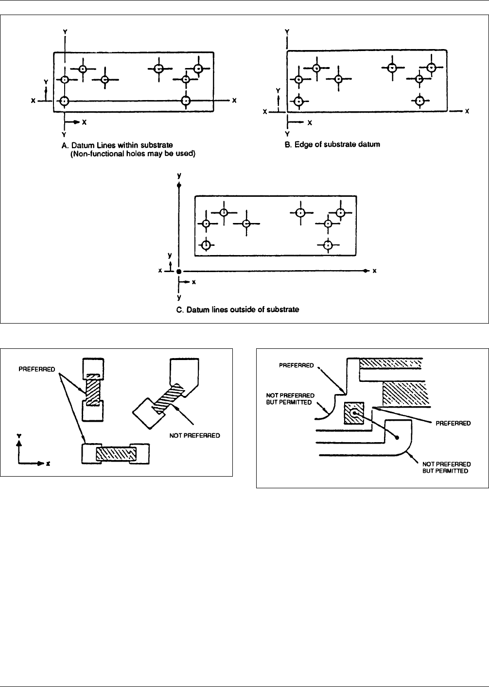
Conductor junctions, the corners of mounting lands and conductor-resistor patterns should be designed with right- angled edges and turns as shown in Figure 5–5. Rounded corners, which can be generated when photoplotters …

Generally, the hybrid designer should make certain that his
selection of materials is:
• physically capable of supporting the components and,
• sufficiently thick to withstand shock and vibration
requirements (varies with size).
Finally, design outlines should be of simple geometries
such as orthogonal quadrilaterals or circles. Designs which
employ sharp internal corners should be avoided because
of the stress risers they present and the greater potential for
breakage.
5.2.1.1 Material Size Considerations While multilayer
hybrid substrates of up to 19,350 sq. mm [30 sq. in.] have
been successfully fabricated, the designer must keep in
mind the normal limitations of equipment use in both the
fabrication and assembly of multilayer hybrid circuits. It is
recommended that the designer check with his fabricators
and assemblers before embarking on a design of unusual
dimensions.
The lidding of packages is also a concern. Lids on metal
cans not only hermetically seal the hybrid but can act as a
mechanical reinforcement. However, if the hybrid is exces-
sively large or of a poorly chosen material, the heat of sol-
dering on the lid can result in a latent mismatch in CTE
stressing the device and making it subject to failure by
either cracking of the substrate or popping off of the lid.
5.2.1.2 Quality Conformance Test Coupons Test cou-
pons, when required for process/quality control, are situ-
ated in such a manner that they are representative of the
board processing; are characteristic of the product, and
meet the requirements of IPC-HM-860.
5.2.2 Dimensions and Tolerances Where appropriate,
dimensions and tolerances shall be in accordance with
IPC-D- 300.
5.2.3 Datums Datums shall meet the requirements of
paragraph 3.3.6 (See Figure 5–3 for the establishment of
datum references.)
5.2.4 Thickness Considerations Symmetrical construc-
tions play a major role in allowing a hybrid manufacturer
the ability to minimize bow. Constructions which are
asymmetric induce greater warpage. Finished circuits
should have a minimum of 0.035 mm [0.0014 inch] of
dielectric material between conductive layers.
Overall thickness shall include metallic deposition and
shall be specified on the master drawing. In critical areas,
such as connector contact areas, the thickness tolerances
may be more stringent and shall be detailed on the master
drawing, and should, wherever possible be limited only to
those areas where needed.
In order to allow the manufacturer to use the most
dimensionally-stable and cost-effective materials for their
process, the designer minimizes the number of tolerances
invoked on the lay-up. In general, the following toleranc-
ing is appropriate:
Class A—A tolerance should only be placed on the overall
thickness.
Class B—A tolerance should only be placed on the overall
thickness and on the dimensions between a few selected
layers.
Class C—Tolerances can be placed on all of the spaces
between layers. A tolerance can also be placed on the over-
all thickness if the tolerance is sufficiently large to accom-
modate the accumulation of the tolerances between layers.
If the overall thickness tolerance is not sufficiently large,
the manufacturer might not be able to fabricate the circuit
or he may be required to selectively choose the materials
for the lay-up, which is very expensive.
5.2.5 Substrate Edges One substrate edge should be
located from a datum and, where applicable, other edges
should be dimensioned from that same datum.
5.3 Circuit Features
5.3.1 Conductors
Conductors on the hybrid circuit may
take a variety of shapes, they may be in the form of single
conductor traces, or conductor planes.
Due to screen printing variables and conductor flow-out
after printing, processing allowances should be built into
the design, to allow the manufacturer to produce a part that
will meet the end-product requirements detailed on the
master drawing. For a typical high resolution conductor,
the width of the screen pattern will be 0 to 25 µm smaller
than the corresponding width specified for the fired film.
Conductors without high resolution properties may require
the allowance to be as great as 50 µm.
5.3.1.1 Conductor Width and Thickness The width and
thickness of conductors on the finished circuit shall be
determined on the basis of the current-carrying capacity
required, and the allowable temperature rise.
For ease of manufacturing and durability in usage, conduc-
tor width and spacing requirements should be maximized
while maintaining the minimum spacing requirements of
Table 3–1.
5.3.1.2 Conductor Routing The length of a conductor
between any two terminal areas should be held to a mini-
mum.
Conductor and resistor patterns should be oriented in the
‘‘X’’ and ‘‘Y’’ axes as shown in Figure 5–4.
December 1989 IPC-D-859
43
Conductor junctions, the corners of mounting lands and
conductor-resistor patterns should be designed with right-
angled edges and turns as shown in Figure 5–5. Rounded
corners, which can be generated when photoplotters are
used for artwork, are not preferred but are permitted.
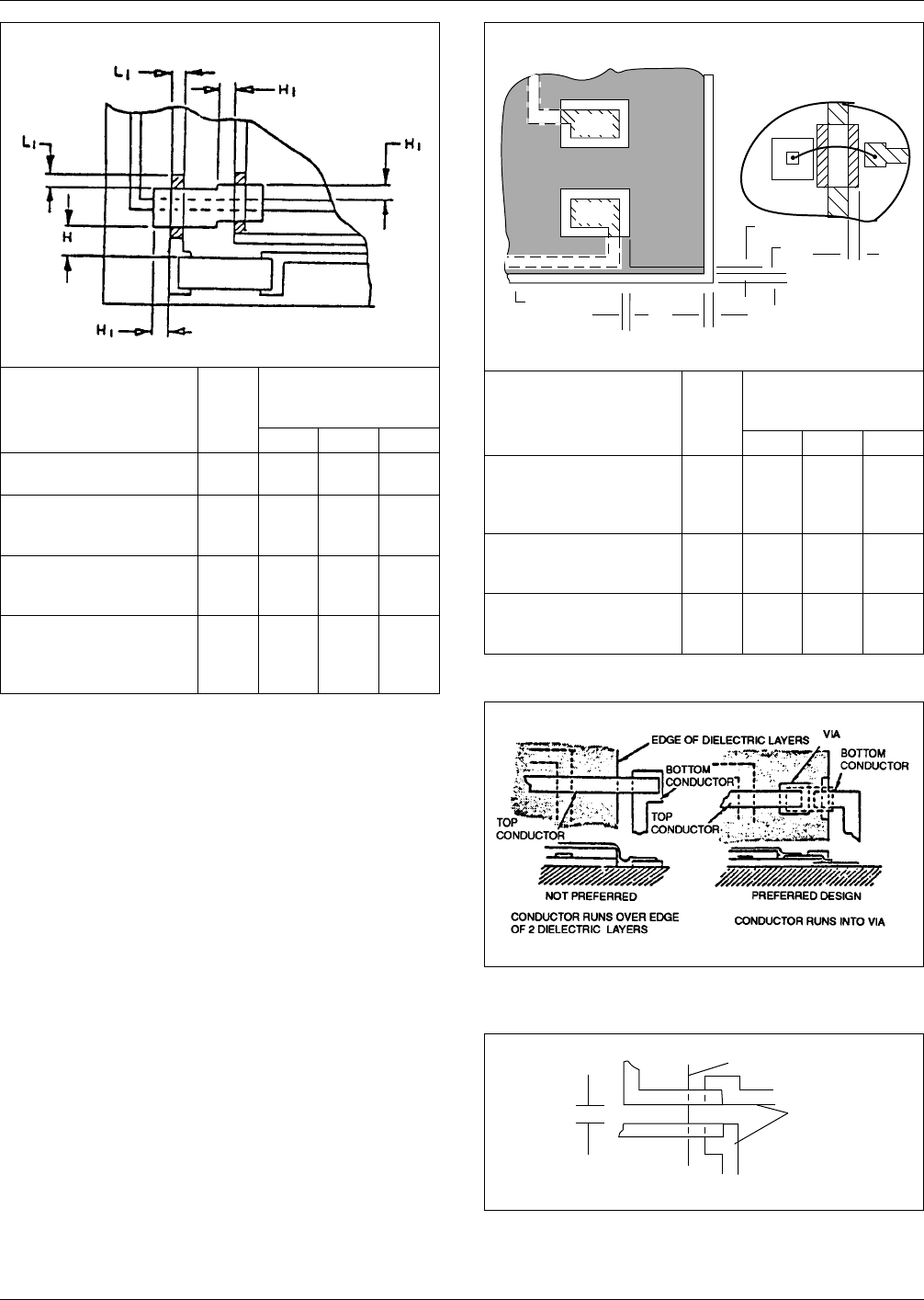
5.3.1.3 Conductor Spacing Minimum conductor spac-
ing shall be in accordance with Table 3–1 and Figures 5–6
and 5–7.
5.3.1.4 Conductor Layout Guidelines The following
guidelines should be observed during the layout of thick-
film multilayer circuits:
A. Avoid running conductors over the edge of multiple
dielectric layers; use vias (see Figure 5–8).
B. The spacing between conductors must be a minimum of
0.38 mm [0.015 inch] if it is necessary to run conduc-
tors over the edge of a single dielectric layer (see Fig-
ure 5–9).
C. Avoid running conductors parallel to other conductors
that are directly beneath them for long distances (see
Figure 5–10).
D. An overlap at least 0.25 mm [0.010 inch] is recom-
mended where a top and bottom conductor connect to
one another (see Figure 5–11).
IPC-859-5-3
Figure 5–3 Establishing datums
IPC-859-5-4
Figure 5–4 Orientation for conductor–resistor patterns
IPC-859-5-5
Figure 5–5 Land and conductor geometries
IPC-D-859 December 1989
44
E. The maximum number of conductor levels for high
yields is three. Processing yields may be affected with
additional layers, although an infinite number of layers
are theoretically possible.
F. Semiconductor chips, capacitor chips, and resistor
chips may be mounted on lands on the top conductor
level of multilayer thick-film designs. Also, ultrasonic
wire bonds may be made from the chips to the lands;
however, it is recommended that thermo-compression
bonds be made only to bottom level conductors. If
thermo-compression bonds must be made to the top
conductor level, a double conductor layer should be
used for the land (see Figure 5–12)
G. Provide test points for short-circuit and continuity
checking between conductor levels.
5.3.2 General Requirements for Lands and Bond Lands
The following general requirements shall be met for all
lands and bond lands.
IPC-859-5-6
Dim
Producibility mm
[inch]
Most ↔ Least
ABC
Resistor
distance to dielectric
H 1.27
[0.050]
1.14
[0.045]
1.14
[0.045]
Conductor lines staggered,
1
distance to dielectric step
(typical on 2-layer circuit).
H
1
0.51
[0.020]
0.38
[0.015]
0.25
[0.010]
Conductor lines overlap
L
1
0.38x
0.38
[0.015]
0.25x
0.25
[0.010]
0.25x
0.25
[0.010]
Dielectric crossover,
distance extended beyond
width (on either top or
bottom conductor).
H
1
0.51
[0.020]
0.38
[0.015]
0.38
[0.015]
1. A staggered dielectric configuration is required whenever two (closely
placed) adjacent conductors are screened over a dielectric crossover.
Figure 5–6 Minimum dielectric distance from other lines
and for crossovers.
IPC-859-5-7
Dim
Producibility mm
[inch]
Most ↔ Least
ABC
Dielectric distance to
metallized land for solder
or epoxy component
attachment.
W 0.38
[0.015]
0.25
[0.010]
0.25
[0.010]
Dielectric distance to edge
of substrate, minimum
sized
W
1
0.25
[0.010]
0.13
[0.005]
0.13
[0.005]
Dielectric width, when
covering conductors that
run under bond wire.
W
2
0.25
[0.010]
0.13
[0.005]
0.13
[0.005]
Figure 5–7 Minimum dielectric spacing and size
▼
▼
▼
▼
▼
▼
▼
▼
▼
Substrate
Edge
W
2
W
1
W
1
W
W
2
Solder
Pad
Solder
Pad
▼
▼
DEVICE
IPC-859-5-8
Figure 5–8 Conductor interconnects external to the
dielectric
IPC-859-5-9
Figure 5–9 Spacing between adjacent conductors
running over a dielectric edge.
▼
0.38mm
[0.015"] min.
Dielectric Edge
Bottom
Conductors
▼
▼
▼
▼
December 1989 IPC-D-859
45