IPC-D-859.pdf - 第68页
i. Electrical test requirements. j. Marking requirements. k. Electrostatic discharge protection requirements. The hybrid circuit assembly drawing shall include the defi- nition of any conditions considered in the design w…

paint, the color, and the side(s) of the board to be marked.
If the marking is to be made by silk screen or similar
method, a layout of the marking shall be included as the
last sheet(s) of the artwork master, and shall be referenced
in the marking note.
5.6.1.3 Traceability Marking The master drawing shall
specifically indicate the location for the manufacturer’s
code and all other required traceability markings on the
board. The part number change letter and its location, shall
be indicated on the drawing.
A drawing note shall indicate the acceptable methods of
marking (ink, rubber, stamp, electric pencil, etching, etc.)
and color if applicable.
5.6.2 Assembly Drawing The hybrid circuit assembly
drawing shall cover circuitry on which separately manufac-
tured parts have been added. The hybrid circuit assembly
drawing shall be compatible with IPC-D-325, and may
include at least the following:
a. Parts and material list.
b.Component mounting and installation requirements.
c. Cleanliness requirements.
d.Location and identification of materials.
e. Location and identification of all components.
f. Component orientation and polarity.
g.Applicable ordering data.
h.Structural details when require for support and rigidity.
Table 5–5 Master Drawing Detail Descriptions
A Hybrid Circuit Details 1. The type, size and shape of the hybrid circuit and all tolerance conditions thereof
2. Dielectric separation between layers
3. Bow and twist allowances
4. Overall thickness requirements including tolerances
B Materials 1. Type class and grade of material, including color if appropriate
2. Plating and coating material(s) type and thickness(es)
3. Marking inks or paint and permanency
C Via Details 1. The size, location and tolerances for all vias
D Conductor Definition 1. Shape and arrangement of both conductor and non-conductor patterns on each layer
of the hybrid circuit (copies of the production master(s) or copies of artwork may be
used to define these patterns)
2. Separate views of each conductor layer
3. Dimensions either specifically or by reference to a grid system, for any and all
pattern features not controlled by hole size and location
4. Minimum conductor width and spacing on the finished hybrid circuit
5. Dimensions for critical pattern features which may affect circuit performance because
of distributive inductance or capacitance effects
6. Conductor layer identification
E Marking 1. Hybrid circuit identification marking
2. Size, shape and location of reference designation and legend marking, if required.
3. Serialization and revision level marking
F Processing Conditions 1. Processing allowances that were used in the design of the hybrid circuit, including
but not limited to:
a. Conductor width allowance
b. Conductor spacing allowance
c. Land fabrication allowance
d. Solder mask or cover layer registration allowance
2. Applicable processing specifications
3. Location of quality conformance coupon or circuitry
G Design Concepts 1. Maximum rated voltage (maximum voltage between two non-connected adjacent
conductors with the greatest potential difference
2. Identification of testing and test point location
3. Modular grid system(s) used to identify all holes, test points, lands and overall
dimensions
a. Metric grid—2.0, 1.0, 0.5 or multiples of 0.1 mm
b Inch based grid—0.100, 0.050, 0.025 or multiples of 0.005 inches
(see Section H-3 of this table)
H Documentation Practices 1. All terms used on the master drawing shall conform to this standard and IPC-T-50
2. Notes either included on the first sheet(s) or location of notes specified on the first
sheet(s)
3. Indication of grid using X-Y control dimensions or grid scales. Grids should not be
reproduced on the master drawing to maintain clarity of conductor patterns
December 1989 IPC-D-859
61
i. Electrical test requirements.
j. Marking requirements.
k.Electrostatic discharge protection requirements.
The hybrid circuit assembly drawing shall include the defi-
nition of any conditions considered in the design where the
manufacturing variation between the end product and
assembly configuration play a role in the producibility or
performance of the assembly.
5.6.3 Final Schematic/Logic As a part of the data pack-
age, a final schematic shall also be prepared. The final
schematic shall be back-annotated, so that the reference
designator shown on the assembly drawing and the
schematic/logic diagram agree.
5.6.4 Final Bill of Material A final bill of material shall
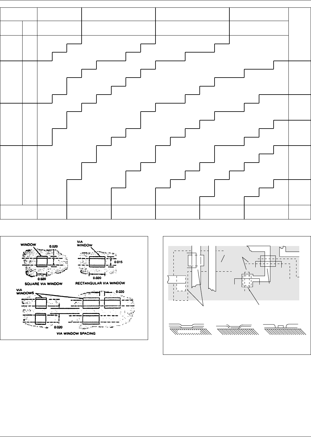
Power (MW)
Dissipation →
0–100 100–150 150–200 200–250
↓
W
L
1.02 1.14 1.27 1.4 1.52 1.65 1.78 1.91 2.03 2.16 2.29 2.41 2.54 2.67 2.79 2.92 3.05
0–100
1.02 1.000 0.888 0.800 0.727 0.666 0.615 0.571 0.533 0.500 0.470 0.444 0.421 0.400 0.380 0.363 0.347 0.333
200–3001.14 1.125 1.000 0.900 0.818 0.750 0.692 0.642 0.600 0.562 0.529 0.500 0.473 0.450 0.428 0.409 0.391 0.375
1.27 1.250 1.111 1.000 0.909 0.833 0.769 0.714 0.666 0.625 0.588 0.555 0.526 0.500 0.476 0.454 0.434 0.416
100–150
1.4 1.375 1.222 1.100 1.000 0.916 0.846 0.785 0.733 0.687 0.647 0.611 0.578 0.550 0.523 0.500 0.478 0.458
300–400
1.52 1.500 1.333 1.200 1.090 1.000 0.923 0.857 0.800 0.750 0.705 0.666 0.631 0.600 0.571 0.545 0.521 0.500
1.65 1.825 1.444 1.300 1.181 1.083 1.000 0.928 0.866 0.812 0.764 0.722 0.684 0.650 0.619 0.590 0.565 0.541
1.78 1.750 1.555 1.400 1.272 1.166 1.076 1.000 0.933 0.875 0.823 0.777 0.736 0.700 0.666 0.636 0.608 0.583
1.91 1.875 1.666 1.500 1.363 1.250 1.153 1.071 1.000 0.937 0.882 0.833 0.789 0.750 0.714 0.681 0.652 0.625
400–500
150–200
2.03 2.000 1.777 1.600 1.454 1.333 1.230 1.142 1.066 1.000 0.941 0.888 0.842 0.800 0.761 0.727 0.695 0.666
2.16 2.125 1.888 1.700 1.545 1.416 1.307 1.214 1.133 1.062 1.000 0.944 0.894 0.850 0.809 0.772 0.739 0.708
2.29 2.250 2.000 1.800 1.636 1.500 1.384 1.285 1.200 1.125 1.058 1.000 0.947 0.900 0.857 0.818 0.782 0.750
500–6002.41 2.375 2.111 1.900 1.727 1.583 1.461 1.357 1.266 1.187 1.117 1.055 1.000 0.950 0.904 0.863 0.826 0.791
2.54 2.500 2.222 2.000 1.818 1.666 1.538 1.428 1.333 1.250 1.176 1.111 1.052 1.000 0.952 0.909 0.869 0.833
200–300
2.67 2.625 2.333 2.100 1.909 1.750 1.615 1.500 1.400 1.312 1.235 1.166 1.105 1.050 1.000 0.954 0.913 0.875
600–700
2.79 2.750 2.444 2.200 2.000 1.833 1.692 1.571 1.466 1.375 1.294 1.222 1.157 1.100 1.047 1.000 0.956 0.916
2.92 2.875 2.555 2.300 2.090 1.916 1.769 1.642 1.533 1.437 1.352 1.277 1.210 1.150 1.095 1.045 1.000 0.958
3.05 3.000 2.666 2.400 2.181 2.000 1.846 1.714 1.600 1.500 1.411 1.333 1.263 1.200 1.142 1.090 1.043 1.000
3.18 3.125 2.777 2.500 2.272 2.083 1.923 1.785 1.666 1.562 1.470 1.388 1.315 1.250 1.190 1.136 1.086 1.041
700–8003.30 3.250 2.888 2.600 2.363 2.166 2.000 1.857 1.733 1.625 1.529 1.444 1.368 1.300 1.238 1.181 1.130 1.083
3.43 3.375 3.000 2.700 2.454 2.250 2.076 1.928 1.800 1.687 1.588 1.500 1.421 1.350 1.285 1.227 1.173 1.125
200–300 300–400 400–500 500–600 600–700 700–800
Figure 5–40 Thick-film resistor length-width-power
IPC-859-5-41
Figure 5–41 Nominal via window dimensions
IPC-859-5-42
Figure 5–42 Illustration of various multilayer via designs
▼
▼
▼
▼
▼
▼▼
▼
▼▼
▼
▼
Bottom
Conductor
Via window larger than
bottom conductor but
smaller than top con-
ductor
▼
Via window smaller than
bottom conductor but larger
than top conductor
Via window larger than
bottom conductor but
smaller than top conductor
Substrate
A
A
B
C
B
C
Section thru A-A Section thru B-B Section thru C-C
IPC-D-859 December 1989
62
be prepared as a part of the drawing package. This final bill
may be a computer listing, or may be in drawing format.
6.0 Quality Assurance This section provides require-
ments and considerations for the quality and quality assur-
ance provisions that incorporate test coupons into the board
design. This section also includes a brief discussion of
bare-board testing.
6.1 General Quality concepts should be included in all
aspects of the hybrid circuit design. Quality considerations
apply to manufacture, assembly and bare board assembly
testing. The design concepts are the key to the capability of
achieving quality in the previously mentioned areas. Good
workmanship insures that quality. In lieu of test coupons,
production boards may be employed in tests used to deter-
mine the acceptability of hybrid circuits.
6.2 Bare Board Testing Bare board testing is an electri-
cal evaluation of the completely fabricated end-product cir-
cuit without components. Electrical checks are made for
point-to-point continuity, low resistance (opens), and high
resistance (shorts).
Visual surface characteristics may be verified using auto-
matic optical inspection.
6.2.1 Approaches There are two approaches to bare
board testing, namely:
A. Test all lands.
B. Test for opens at low-voltage levels, and test for shorts
at high-voltage levels.
6.3 Design Considerations
6.3.1 Lands On Grid
All lands to be involved in bare
board testing shall be on grid, so that universal test fixtures
can be used. (Commonly used grids are 2.54 mm [0.100
inch] and 1.27 mm [0.050 inch].)
6.3.2 Lands Off Grid If the conditions in 6.4.2.1 are not
possible, the board layout should attempt to limit the
required number of off-grid lands, so that test fixtures with
flexible pins may be used, or so that a dedicated test fix-
ture can be made cost-effectively.
6.3.3 Power-to-Ground Measurement Information
should be on the initial design documentation that indicates
lands for measuring power-to-ground relationships.
6.4 Test Tapes Test tapes should be generated from
known, good circuits.
6.5 Test Circuitry Quality conformance testing may be
done on the finished part, or quality conformance test cir-
cuitry, or a combination of both.
The coupons should be produced on separate substrates;
however, all coupons required shall be shown on the mas-
ter drawing artwork and the production master. Figure 6–1
shows the individual coupon layout for layer 1, and Figure
6–7 depicts artwork configuration for layers 1 through 10.
Dimensions shown in Figures 6–2 through 6–6 apply to all
layers.
Special test coupons F through L are shown in Figures 6–8
through 6–13. These may be used for additional testing as
indicated, at the designer’s discretion; however, when their
use is specified, they shall also be shown on the master
drawing artwork and the production master.
6.5.1 Quantity At least one complete set of quality con-
formance test circuitry (coupons A through E) shall be pro-
vided with each lot of each part number produced.
6.5.2 Manufacturing Requirements The coupons shall
be fired under normal furnace loading conditions. They
shall be processed utilizing the same production equip-
ment, procedures, and personnel used in regular produc-
tion. Operations shall be divided up betweeen identical or
similar types of equipment, operating shifts, and personnel;
and all coupons shall be totally representative of the prod-
uct.
6.5.3 Identification The coupons are to be identified
with the following:
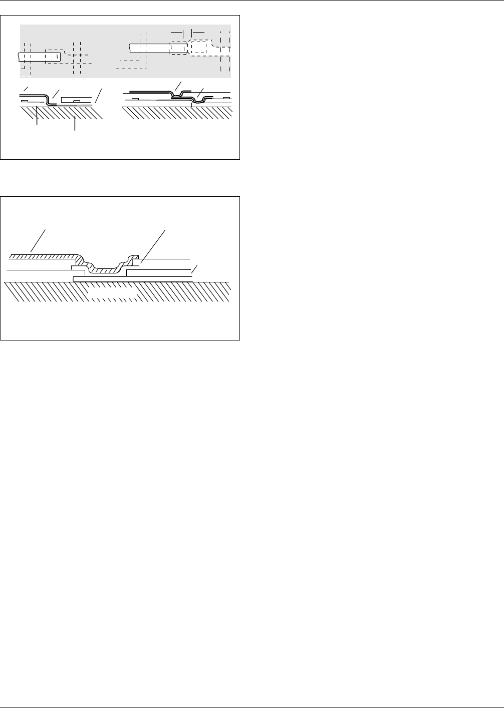
IPC-859-5-43
Figure 5–43 Routing conductors through multiple
dielectric layers
▼
▼
▼
▼
▼
▼
▼
▼
▼
VIA
VIA
SUBSTRATE
VIA
TOP LEVEL
SECOND LEVEL
NOT PREFERRED
VIAS NOT STAGGERED
PREFERRED DESIGN-
VIAS ARE STAGGERED
BOTTOM LEVEL
IPC-859-5-44
Figure 5–44 Use of a blind through-hole land
Substrate
Top Conductor Blind Land on
Second Level
Bottom
Conductor
▼
▼
▼
December 1989 IPC-D-859
63