CMV12000_DS000603_6-00.pdf - 第20页
Document Feedback CMV12000 Functional Description Datasheet • PUBLIC DS000603 • v6 - 00 • 2023 -Sep- 22 84 │ 19 7 Functional Description 7.1 Sensor Architecture Figure 2 shows the image sen sor architecture. The internal…
Document Feedback
CMV12000
Typical Operating Characteristics
Datasheet • PUBLIC
DS000603 • v6-00 • 2023-Sep-22
84 │ 18
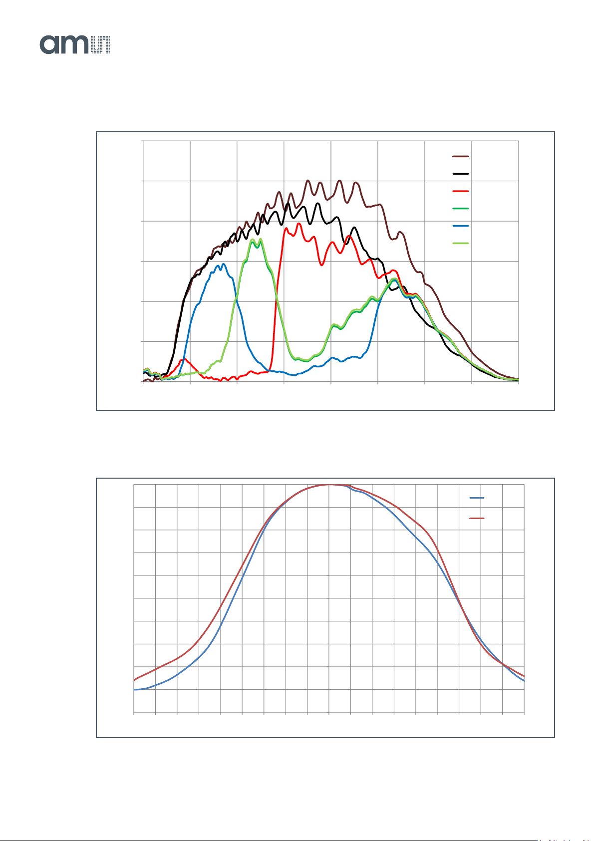
Figure 9:
Spectral Response
Figure 10:
Angular Response
0
0.05
0.1
0.15
0.2
0.25
0.3
300 400 500 600 700 800 900 1000 1100
Spectral response [A/W]
Wavelength [nm]
NIR
Mono
Color_R
Color_Gr
Color_B
Color_Gb
0
10
20
30
40
50
60
70
80
90
100
-45 -40 -35 -30 -25 -20 -15 -10 -5 0 5 10 15 20 25 30 35 40 45
Relative response [%]
Incmoming light angle [°]
Vertical
Horizontal

Document Feedback
CMV12000
Functional Description
Datasheet • PUBLIC
DS000603 • v6-00 • 2023-Sep-22
84 │ 19
7 Functional Description
7.1 Sensor Architecture
Figure 2 shows the image sensor architecture. The internal sequencer generates the necessary
signals for image acquisition. The image is stored in the pixel (global shutter) and they are read out
sequentially, row-by-row. On the pixel output, an analog gain is possible. The pixel values then passes
to a column ADC cell, in which ADC conversion is performed. The digital signals are then read out
over multiple LVDS channels. Each LVDS channel reads out 128 adjacent columns of the array. The
read-out of the pixel array is performed on both sides (top and bottom) of the pixel array to speed up
the read-out process and achieve the frame rate of 300 fps at full resolution and 10-bit. In each line
read-out cycle, two lines are selected for read-out. In the Y-direction, rows of interest are selected
through a row-decoder, which allows a flexible windowing. Control registers are foreseen for the
programming of the sensor. These register parameters are uploaded via a four-wire SPI interface. A
temperature sensor, which can be read out over the SPI interface, is also included.
7.1.1 Pixel Array
The pixel array consists of 4096 x 3072 square global shutter pixels with a pitch of 5.5 μm (5.5 μm x
5.5 μm). This results in an optical area of 22.5 mm x 16.9 mm (28.1 mm diameter).
The pixels are designed to achieve maximum sensitivity with low noise (using CDS) and low PLS
specifications. Micro lenses are placed on top of the pixels for improved fill factor and quantum
efficiency.
There are 16 dark reference columns available on the sensor (columns 0 to 7 and 4088 to 4095)
which can be enabled/disabled by programming the appropriate sensor register.
7.1.2 Analog Front End
The analog front end consists of two major parts, a column amplifier block and a column ADC block.
The column amplifier prepares the pixel signal for the column ADC and applies analog gain if desired
(programmable using the SPI interface). The column ADC converts the analog pixel value to an 8-, 10-
or 12-bit value and can apply a gain. A digital offset can also be applied to the output of the column
ADCs. All gain and offset settings can be programmed using the SPI interface.
7.1.3 LVDS Block
The LVDS block converts the digital data coming from the column ADC into standard serial LVDS data
running at maximum 600 Mbit/s. The sensor has 66 LVDS output pairs:

Document Feedback
CMV12000
Functional Description
Datasheet • PUBLIC
DS000603 • v6-00 • 2023-Sep-22
84 │ 20
● 64 Data channels
● 1 Control channel
● 1 Clock channel
The 64 data channels are used to transfer 8-bit, 10-bit or 12-bit data words from sensor to receiver.
The output clock channel transports a DDR clock (max 300 MHz), synchronous to the data on the
other LVDS channels. This clock can be used at the receiving end to sample the data. The data on the
control channel contains status information on the validity of the data on the data channels, among
other useful sensor status information. Details on the LVDS timing and format can be found in section
7.3 of this document.
7.1.4 Sequencer
The on-chip sequencer will generate all required control signals to operate the sensor from only a few
external control signals. This sequencer can be activated and programmed through the SPI interface.
7.1.5 SPI Interface
The SPI interface is used to load the sequencer registers with data. The data in these registers is used
by the sequencer while driving and reading out the image sensor. Features like windowing,
subsampling, gain and offset are programmed using this interface. The data in the on-chip registers
can also be read back for test and debug of the surrounding system.
7.1.6 Temperature Sensor
A 16-bit digital temperature sensor is included in the image sensor and can be controlled by the SPI-
interface. The on-chip temperature can be obtained by reading out the register with address 127.
7.2 Operating the Sensor
This section explains how to connect and power the sensor, as well as basic recipes of how to
configure the sensor in a certain operation mode.
Information
All register values are in decimal notation unless otherwise specified.
7.2.1 Power Supplies
To power the sensor, five externally generated supplies are required (VDD18, VDD33, VDD_PIX and
VDD_RES).