CMV12000_DS000603_6-00.pdf - 第69页
Document Feedback CMV12000 Functional Description Datasheet • PUBLIC DS000603 • v6 - 00 • 2023 -Sep- 22 84 │ 68 Mode Number of Outputs Per Side Reg. Address 32 16 8 4 2 1 114 200 200 200 200 200 200 X&Y-Subsampling 8…
Document Feedback
CMV12000
Functional Description
Datasheet • PUBLIC
DS000603 • v6-00 • 2023-Sep-22
84 │ 67
Mode
Number of Outputs Per Side
Reg. Address
32
16
8
4
2
1
113
798
1586
1586
1586
1586
1586
114
90
109
109
109
109
109
Binning
82
798
798
798
542
286
286
83
5894
5894
5894
5898
5908
5908
84
575
575
575
575
575
575
85
575
575
575
1031
2063
4127
86
143
143
143
257
515
1031
87
630
630
630
630
630
630
88
630
630
630
630
630
630
98
36619
36619
36619
36619
36619
36619
107
11606
11606
11606
11606
11606
11606
109
13416
13416
13416
13416
13416
13416
113
1054
1054
1054
1054
1054
1054
114
100
100
100
100
100
100
7.7.3 12b Mode
These settings need to be adjusted per number of channels used per side and normal, X&Y-
subsampling or binning mode.
Figure 93:
Additional Required Settings for 12b Mode
Mode
Number of Outputs Per Side
Reg. Address
32
16
8
4
2
1
Normal Mode
82
1822
1822
1054
542
286
286
83
5897
5897
5897
5897
5897
5897
84
244
257
257
257
257
257
85
244
257
515
1031
2063
4127
86
244
257
515
1031
2063
4127
87
1910
1910
1910
1910
1910
1910
88
1910
1910
1910
1910
1910
1910
98
39433
39433
39433
39433
39433
39433
107
11102
11102
11102
11102
11102
11102
109
14835
14448
14448
14448
14448
14448
113
534
542
542
542
542
542

Document Feedback
CMV12000
Functional Description
Datasheet • PUBLIC
DS000603 • v6-00 • 2023-Sep-22
84 │ 68
Mode
Number of Outputs Per Side
Reg. Address
32
16
8
4
2
1
114
200
200
200
200
200
200
X&Y-Subsampling
82
2078
3102
1054
542
286
286
83
5893
5893
5893
5893
5893
5893
84
239
257
257
257
257
257
85
239
257
515
1031
2063
4127
86
119
128
257
515
1031
2063
87
1975
1935
1935
1935
1935
1935
88
1975
1935
1915
1915
1915
1915
98
36364
36364
36364
36364
36364
36364
107
11102
11102
11102
11102
11102
11102
109
14835
14835
14835
14835
14835
14835
113
529
542
542
542
542
542
114
190
200
200
200
200
200
Binning
82
1054
1054
1054
542
286
286
83
5893
5893
5893
5898
5898
5898
84
479
479
479
479
479
479
85
479
479
515
1031
2063
4127
86
119
119
128
257
515
1031
87
1255
1255
1425
1425
1425
1425
88
1255
1255
1425
1425
1425
1425
98
36620
36620
36620
36620
36620
36620
107
11102
11102
11102
11102
11102
11102
109
14835
14835
14835
14835
14835
14835
113
13342
13342
9246
7710
7710
7710
114
200
200
200
200
200
200
7.7.4 Clock Speed
Some settings need to be changed depending on the clock speed.
FOT
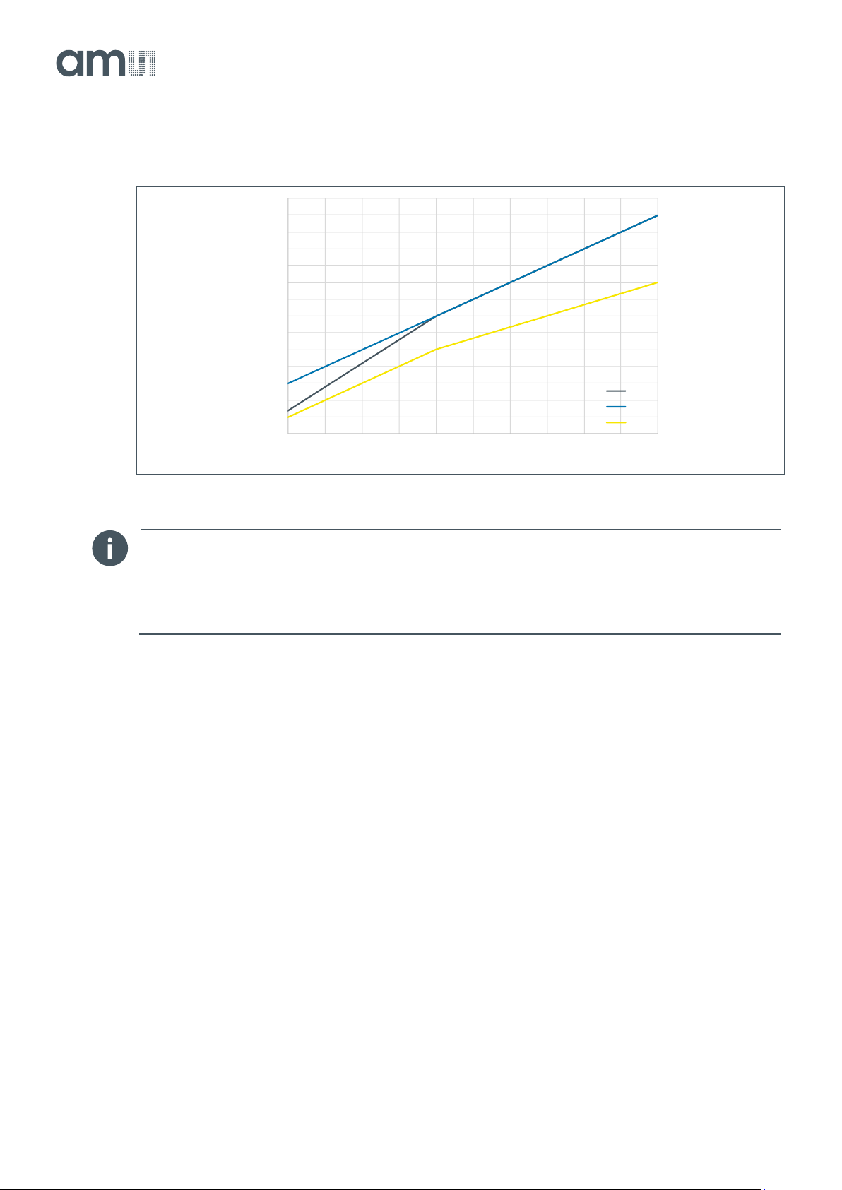
When you are running at a lower speed, register 107[13:7] has to be adjusted to keep the image
quality good. The plots below give you an overview, which value to choose per bit mode. Round down
if the recommended register value is between integers.
Document Feedback
CMV12000
Functional Description
Datasheet • PUBLIC
DS000603 • v6-00 • 2023-Sep-22
84 │ 69
Figure 94:
FOT Register vs Clock Speed
Information
Bits [6:0] of register 107 do not change with clock speed. Keep these bits always the same, at the
recommended value from previous sections. For example at 10b default mode, register 107 =
11614, so bits [6:0] should remain 94.
ADC Range
The ADC range is dependent of the input clock speed, the slower the clock the higher the ADC range
setting has to be. Below you can see a plot showing which ADC range and multipliers to use with a
certain clock speed and bit mode.
The multiplier registers set the total multiplication for the ADC input range. The table below gives an
overview of the total multiplication (used in Figure 96) that is applicable.
For example, when running at 400 MHz, make a vertical line on this frequency until crossing all 3
diagonal lines. Crossing the dashed yellow line, this refers to 12b_mult_x16. Then, find x16 on the
table from Figure 95, finally, you should use the values:
● ADC_range = 70, ADC_range_mult = 3, ADC_range_mult2 = 3 for 12b ADC.
● ADC_range = 220, ADC_range_mult = 1, ADC_range_mult2 = 0 for 10b ADC.
● ADC_range = 247, ADC_range_mult = 0, ADC_range_mult2 = 0 for 8b ADC.
77
78
79
80
81
82
83
84
85
86
87
88
89
90
91
100 150 200 250 300 350 400 450 500 550 600
Reg107[13:7]
LVDS Input CLK [MHz]
FOT register vs CLK
8b
10b
12b