CMV12000_DS000603_6-00.pdf - 第22页
Document Feedback CMV12000 Functional Description Datasheet • PUBLIC DS000603 • v6 - 00 • 2023 -Sep- 22 84 │ 21 It is recommended to decouple ev ery physical supply pin at the sensor with a 100 nF ceramic capacitor per p…

Document Feedback
CMV12000
Functional Description
Datasheet • PUBLIC
DS000603 • v6-00 • 2023-Sep-22
84 │ 20
● 64 Data channels
● 1 Control channel
● 1 Clock channel
The 64 data channels are used to transfer 8-bit, 10-bit or 12-bit data words from sensor to receiver.
The output clock channel transports a DDR clock (max 300 MHz), synchronous to the data on the
other LVDS channels. This clock can be used at the receiving end to sample the data. The data on the
control channel contains status information on the validity of the data on the data channels, among
other useful sensor status information. Details on the LVDS timing and format can be found in section
7.3 of this document.
7.1.4 Sequencer
The on-chip sequencer will generate all required control signals to operate the sensor from only a few
external control signals. This sequencer can be activated and programmed through the SPI interface.
7.1.5 SPI Interface
The SPI interface is used to load the sequencer registers with data. The data in these registers is used
by the sequencer while driving and reading out the image sensor. Features like windowing,
subsampling, gain and offset are programmed using this interface. The data in the on-chip registers
can also be read back for test and debug of the surrounding system.
7.1.6 Temperature Sensor
A 16-bit digital temperature sensor is included in the image sensor and can be controlled by the SPI-
interface. The on-chip temperature can be obtained by reading out the register with address 127.
7.2 Operating the Sensor
This section explains how to connect and power the sensor, as well as basic recipes of how to
configure the sensor in a certain operation mode.
Information
All register values are in decimal notation unless otherwise specified.
7.2.1 Power Supplies
To power the sensor, five externally generated supplies are required (VDD18, VDD33, VDD_PIX and
VDD_RES).

Document Feedback
CMV12000
Functional Description
Datasheet • PUBLIC
DS000603 • v6-00 • 2023-Sep-22
84 │ 21
It is recommended to decouple every physical supply pin at the sensor with a 100 nF ceramic
capacitor per pin. As VDD18 and VDD_PIX draw large peak currents it is also recommended to add a
larger (>10 µF) local capacitor close to the sensor for those supplies. At the voltage regulator side,
also enough bulk decoupling has to be foreseen.
VDD18 draws its peak current every read out line. The peak current decreases with lower data rates.
Care has to be taken in the supply and decoupling design so that VDD18 is always above 1.93 V
during these peaks (so max. 50 mV dip) to guarantee sensor performance. The voltage regulator
should be able to handle the 1.7 A.
VDD_PIX draws a short but large peak current during FOT. Care has to be taken in the supply and
decoupling design so that VDD_PIX is always above 2.9 V during these peaks (so max. 100 mV dip)
to guarantee sensor performance. The peak current should be handled by the decoupling capacitors,
not the voltage regulator.
For VDD33 and VDD_RES the peak currents are lower, but still care has to be taken not allowing the
voltages dips outside the voltage range.
The voltage required is the voltage on the supplies to guarantee the best sensor performance. The
voltage range is the range the voltage should stay within (so during current peaks) to guarantee
sensor performance. If the supply is outside the voltage range, the sensor might still be functional but
performance is not guaranteed. The voltage absolute maximum is the range outside which
(permanent) sensor malfunction might occur.
For more details on the power figures and peak plots, an application note is available. This supply
needs therefore decent decoupling to dampen the current peak.
The sensor will heat up above ambient temperature (+ ~20°C/40°C idle/running at 600 MHz).
Therefore, decent system heat management is needed to keep the sensor junction temperature below
the specifications limit of 70 °C.
7.2.2 Biasing
For optimal performance, some bias pins need to be decoupled to ground or to VDD. Please refer to
the pin list for a detailed description for every pin and the appropriate decoupling.
7.2.3 Digital Input Pins
The table below gives an overview of the external pins used to operate the sensor.
Figure 11:
Digital Input Pins
Pin Name
Description
CLK_IN
Optional input clock, frequency range between 10 MHz and 60 MHz. Only needed for the
internal temperature sensor.
Document Feedback
CMV12000
Functional Description
Datasheet • PUBLIC
DS000603 • v6-00 • 2023-Sep-22
84 │ 22
Pin Name
Description
LVDS_CLK_P/N
Input clock, frequency range between 100 MHz and 600 MHz, depending on the bit mode.
SYS_RES_N
System reset pin, active low signal. Resets the on-board sequencer and must be kept low
during start-up.
FRAME_REQ
Frame request pin. When a high state is detected on this pin, the programmed number of
frames is captured and sent by the sensor. The pulse should be at least 8, 10 or 12 * LVDS
input clock periods wide to be detected, depending on the used bit mode.
SPI_IN
Data input pin for the SPI interface. The data to program the image sensor is sent over this
pin.
SPI_EN
SPI enable pin. When this pin is high, the data should be written/read on the SPI.
SPI_CLK
SPI clock. This is the clock on which the SPI runs (max 30 MHz).
T_EXP1
Input pin, which can be used to program the exposure time externally. The pulse should be
at least 8, 10 or 12 * LVDS input clock periods wide to be detected, depending on the used
bit mode. Optional.
T_EXP2
Input pin, which can be used to program the exposure time externally in interleaved high
dynamic range mode. The pulse should be at least 8, 10 or 12 * LVDS input clock periods
wide to be detected, depending on the used bit mode. Optional.
7.2.4 Clocking
The LVDS input clock defines the output data rate of the CMV12000. The maximum data rate of the
output is 600 Mbit/s (DDR 300 MHz output clock) which results in an input LVDS_CLK clock of
600 MHz. The minimum LVDS_CLK_P/N frequency is 100 MHz for 12-bit, 10-bit and 8-bit. At lower
frequencies, image performance will decrease. Any input frequency (min < f < max) applied (in MHz)
will result in a corresponding output data rate (in Mbit/s). Some register settings need to be changed
when changing the input clock frequency from 600 MHz. See section 7.7.4.
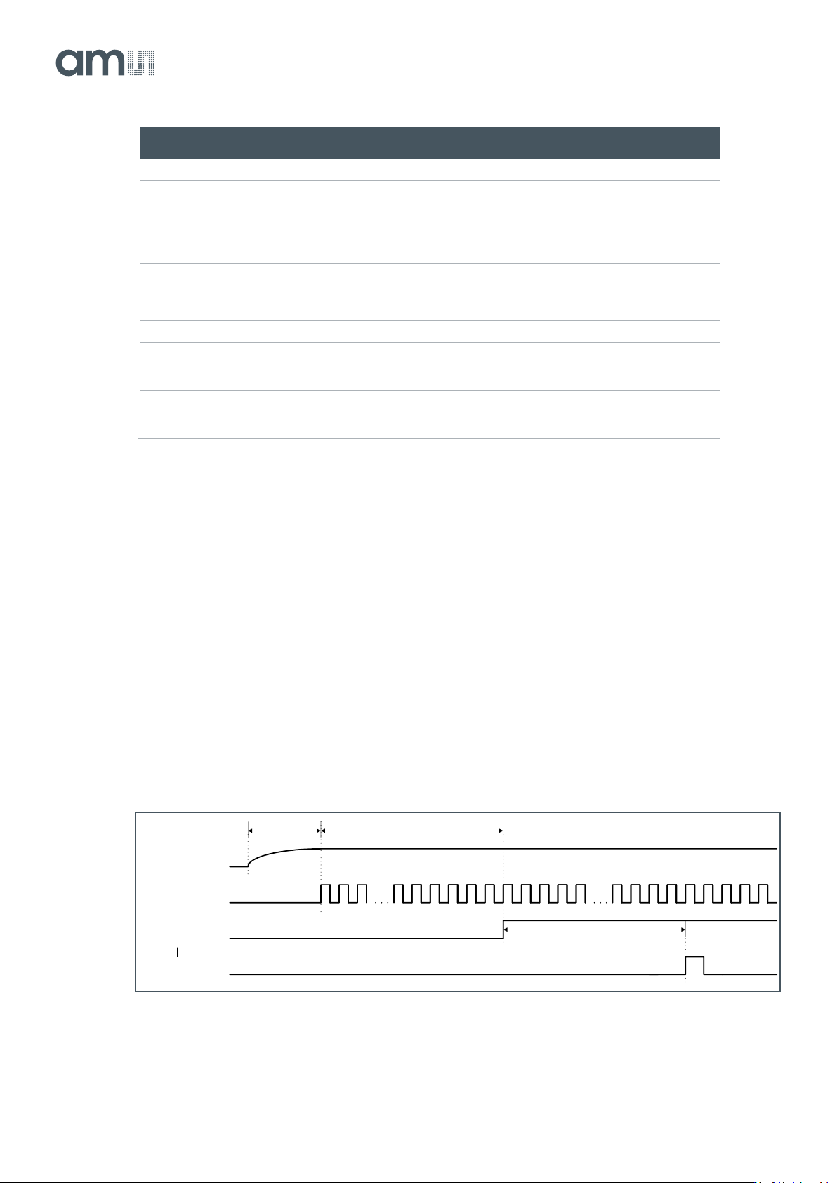
7.2.5 Startup Sequence
The following sequence should be followed when the device is started up:
Figure 12:
Startup Sequence
1μs
1μs
Stable time
Supply
LVDS_CLK
SYS_RES_N
FRAME_REQ