CMV12000_DS000603_6-00.pdf - 第35页
Document Feedback CMV12000 Functional Description Datasheet • PUBLIC DS000603 • v6 - 00 • 2023 -Sep- 22 84 │ 34 Figure 34 : Control Channel Status Bits Bit Function Description [0] DVAL Indicates valid pixel data on the …
Document Feedback
CMV12000
Functional Description
Datasheet • PUBLIC
DS000603 • v6-00 • 2023-Sep-22
84 │ 33
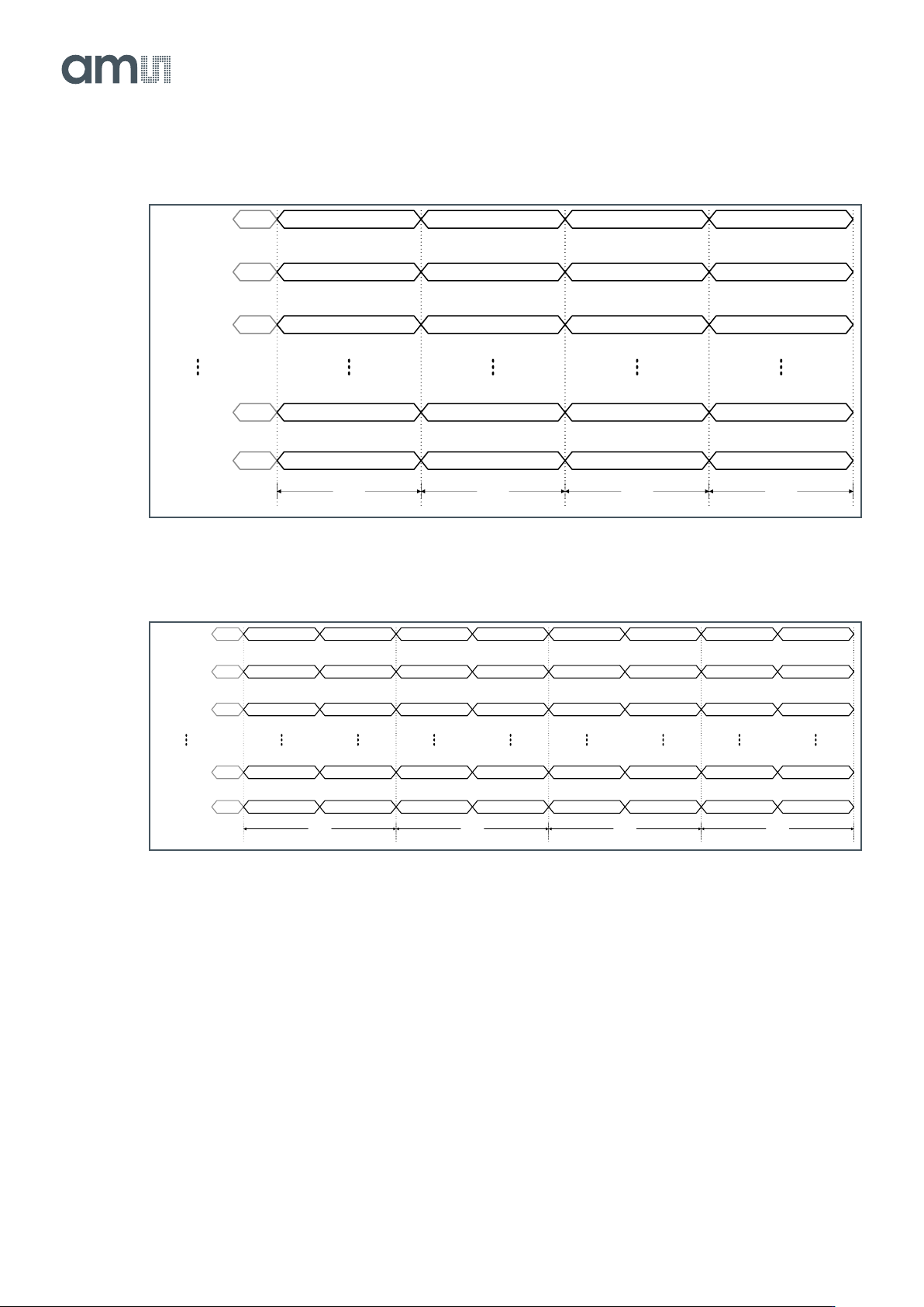
Figure 32:
Pixel Mapping Using 1 × 32 Channels
Figure 33:
Pixel Mapping Using 1 × 16 Channels
7.3.5 Control Channel
The CMV12000 has one LVDS output channel dedicated for the valid data synchronization and timing
of the output channels. The end user must use this channel to know when valid image data or training
data is available on the data output channels.
The control channel transfers status information in 8-bit, 10-bit or 12-bit word format. Every bit of the
word has a specific function. Next table describes the function of the individual bits.
IDLE Pixel 0 to 127Channel 1
IDLEChannel 2
Row 1
Pixel 128 to 255
IDLEChannel 3 Pixel 256 to 383
IDLEChannel 31 Pixel 3840 to 3967
IDLEChannel 32 Pixel 3968 to 4095
Pixel 0 to 127
Row 2
Pixel 128 to 255
Pixel 256 to 383
Pixel 3840 to 3967
Pixel 3968 to 4095
1x32CH
Pixel 0 to 127
Row 4
Pixel 128 to 255
Pixel 256 to 383
Pixel 3840 to 3967
Pixel 3968 to 4095
Pixel 0 to 127
Row 3
Pixel 128 to 255
Pixel 256 to 383
Pixel 3840 to 3967
Pixel 3968 to 4095
IDLE Pixel 0 to 127Channel 1
IDLEChannel 3
Row 1
Pixel 256 to 383
IDLEChannel 5 Pixel 512 to 639
IDLEChannel 29 Pixel 3584 to 3711
IDLEChannel 31 Pixel 3840 to 3967
Pixel 128 to 255
Pixel 384 to 511
Pixel 640 to 767
Pixel 3712 to 3839
Pixel 3968 to 4095
Pixel 0 to 127
Row 2
Pixel 256 to 383
Pixel 512 to 639
Pixel 3584 to 3711
Pixel 3840 to 3967
Pixel 128 to 255
Pixel 384 to 511
Pixel 640 to 767
Pixel 3712 to 3839
Pixel 3968 to 4095
1x16CH
Pixel 0 to 127
Row 4
Pixel 256 to 383
Pixel 512 to 639
Pixel 3584 to 3711
Pixel 3840 to 3967
Pixel 128 to 255
Pixel 384 to 511
Pixel 640 to 767
Pixel 3712 to 3839
Pixel 3968 to 4095
Pixel 0 to 127
Row 3
Pixel 256 to 383
Pixel 512 to 639
Pixel 3584 to 3711
Pixel 3840 to 3967
Pixel 128 to 255
Pixel 384 to 511
Pixel 640 to 767
Pixel 3712 to 3839
Pixel 3968 to 4095
Document Feedback
CMV12000
Functional Description
Datasheet • PUBLIC
DS000603 • v6-00 • 2023-Sep-22
84 │ 34
Figure 34:
Control Channel Status Bits
Bit
Function
Description
[0]
DVAL
Indicates valid pixel data on the outputs
[1]
LVAL
Indicates the validity of the read-out of a row
[2]
FVAL
Indicates the validity of the read-out of a frame
[3]
FOT
Indicates when the sensor is in FOT (sampling of image data in pixels)
(1)
[4]
INTE1
Indicates when pixels of integration block 1 are integrating
(1)
[5]
INTE2
Indicates when pixels of integration block 2 are integrating
(1)
[6]
‘0’
Constant zero
[7]
‘1’
Constant one
[8]
‘0’
Constant zero
[9]
‘0’
Constant zero
[10]
‘0’
Constant zero
[11]
‘0’
Constant zero
(1) These status bits are purely functional and are not required to know if the pixel data is valid. DVAL, LVAL and FVAL is
sufficient to know when to sample the image data.
The status bits of the control channel can be monitored on the TDIG1/2 pins (G26/G27) to see the
state of the sensor. See section 7.6.6 for more details.
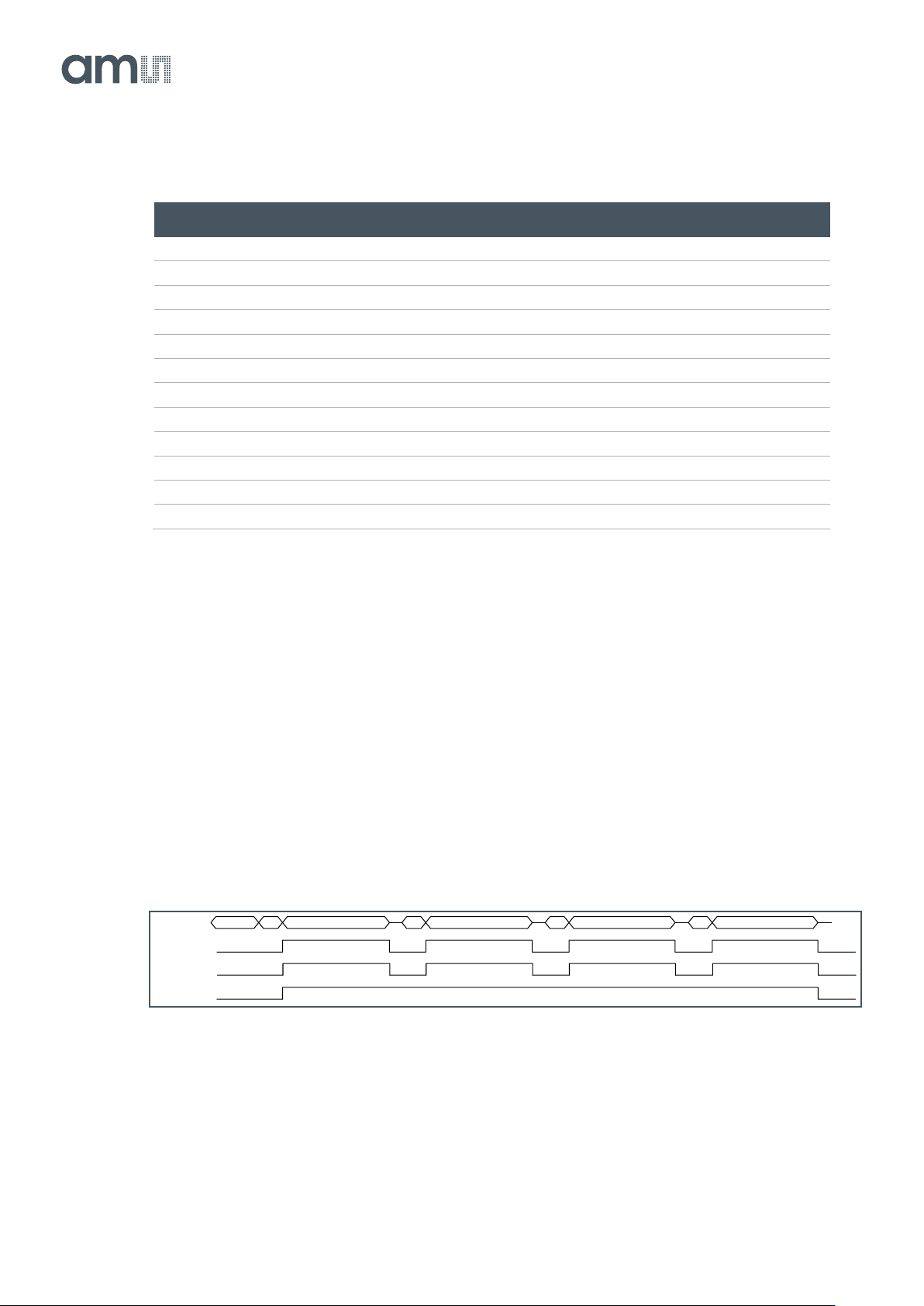
DVAL, LVAL and FVAL
The first three bits of the control word must be used to identify valid data and the read-out status. The
next figure shows the timing of the DVAL, LVAL and FVAL bits of the control channel with an example
of the read-out of a frame of four rows (default is 3072 rows). This example uses the default mode of
64 outputs (identical for one-side 32 outputs).
Figure 35:
xVAL Timing in 2 × 32 Channel Readout Mode
When only 16 outputs are used per side, the line read-out time is two times longer. The control
channel considers this and the timing in this mode looks like the diagram below. The timing
extrapolates identically for 8, 4, 2 and 1 output(s). Below is an example of a frame of two rows when
only using 16 channels per side.
IDLE OH 128 OH 128 OH 128DATA_OUT
DVAL
LVAL
FVAL
OH 128
Document Feedback
CMV12000
Functional Description
Datasheet • PUBLIC
DS000603 • v6-00 • 2023-Sep-22
84 │ 35
Figure 36:
xVAL Timing in 2 × 16 Channel Readout Mode
7.3.6 Training Data
To synchronize the receiving side with the LVDS outputs of the device, a known data pattern can be
put on the output channels. This pattern can be used to “train” the LVDS receiver of the surrounding
system to achieve correct bit and word alignment of the image data. Such a training pattern is set on
all 64 data channel outputs when there is no valid image data to be sent (so, also in between bursts of
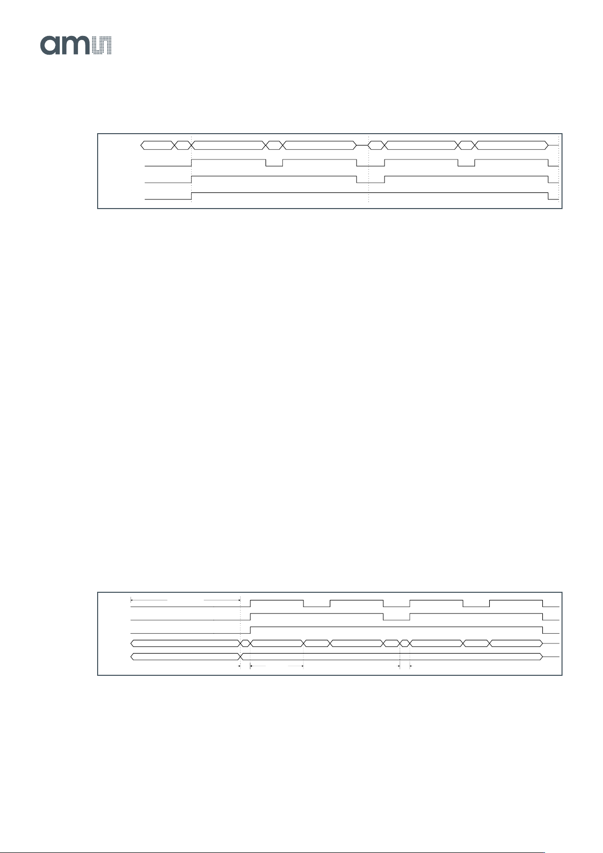
128 pixels). The training pattern is an 8-bit, 10-bit or 12-bit data word that replaces the pixel data. The
sensor has a 12-bit sequencer register (address 89) that can be loaded via SPI to change the contents
of the 12-bit training pattern TP1 for training during idle mode. TP2 equals TP1 with the 8 LSBs
inverted and the 4 MSBs set to ‘0’ and can be used for word alignment during overhead time (OH).
TP2 will be put on the data channels for one bit period and only before every LVAL. When there is
more than one bit of idle time between two LVALs, TP1 will be set on the outputs for the remaining
time. When DVAL is low but LVAL is high, only TP1 will be set on the data outputs.
The control channel does not send a training pattern, because it is used to send control information at
all time. Word alignment can be done on this channel when the sensor is idle (not exposing or sending
image data). In this case, all bits of the control word are zero, except for bit [7] (TPC).
The figure below shows the location of the training pattern on the data channels and control channel
when the sensor is in idle mode and when a frame of two rows is read out. The mode of 16 outputs is
selected.
Figure 37:
TP Timing
The typical output skew of the CMV12000 can be seen below. Per channel per side there is about a
150 ps skew, which leads to a total skew of 4650 ps between the first and lasts channels (OUT1 to
OUT32 and OUT33 to OUT64). TP1 and TP2 can be used to correct for this during operation. The
skew is independent of the clock speed, but shifts with temperature. Therefore, realignment is needed
IDLE OH 128 OH 128 OH 128DATA_OUT
DVAL
LVAL
FVAL
OH 128
TP1 TP2 TP1 TP2
Data
channels
DVAL
LVAL
FVAL
Control
channel
TPC Control information
Sensor in idle mode
TP1 Pixel dataTP1 Pixel dataPixel dataPixel data
128 clock cycles1 clock cycle 1 clock cycle