CMV12000_DS000603_6-00.pdf - 第62页
Document Feedback CMV12000 Functional Description Datasheet • PUBLIC DS000603 • v6 - 00 • 2023 -Sep- 22 84 │ 61 7.6.3 Electrical Black Reference Columns The first and last eight columns of the pixel array can be changed …
Document Feedback
CMV12000
Functional Description
Datasheet • PUBLIC
DS000603 • v6-00 • 2023-Sep-22
84 │ 60
7.6 Additional Features
7.6.1 Offset
A digital offset can be applied to the output signal. This dark level offset can be programmed by setting
the desired value in the sequencer registers. A bottom and top channel offset can be given to the dark
level by programming the appropriate registers. This offset should be adjusted per device and per bit
mode to get the desired dark level.
Figure 81:
Offset Settings
Reg. Name
Address
Bits
Default
Description
Offset_bot
87
[11:0]
780
Sets the relative offset of the dark level for the bottom
outputs following a 2’s-complement code.
1815: 12b
510: 10b
520: 8b
Offset_top
88
[11:0]
780
Sets the relative offset of the dark level for the top
outputs following a 2’s-complement code.
1815: 12b
510: 10b
520: 8b
7.6.2 Gain
An analog (using a Programmable Gain Amplifier) and digital gain (after ADC) can be applied to the
image. The digital gain has to be adjusted based on the bit mode for a unity gain.
Figure 82:
Gain Settings
Reg. Name
Address
Bits
Default
Description
PGA_gain
115
[2:0]
0
0: x1
1: x2
3: x3
7: x4
PGA_div
115
[3]
0
Can be used in binning mode
0: Divide by 1
1: Divide by 3
Dig_gain
117
[4:0]
4
Set to 1,2,3,4,6,8,10,12,14,16 to get the appropriate
digital gain. For unity gain use:
1: 12b
4: 10b
6: 8b
Document Feedback
CMV12000
Functional Description
Datasheet • PUBLIC
DS000603 • v6-00 • 2023-Sep-22
84 │ 61
7.6.3 Electrical Black Reference Columns
The first and last eight columns of the pixel array can be changed to an electrical black reference. This
electrical black reference can be used to correct row noise. The black level offset between the EB and
normal pixels will differ. Because of the limited amount of EB pixels per row (16), row correction is
limited.
Figure 83:
Electrical Black Reference Settings
Reg. Name
Address
Bits
Default
Description
Black_col_en
89
[15]
0
0: Off
1: On
7.6.4 Test Pattern
The sensor has a built-in digital fixed test pattern. This can be used, for example, to test the FPGA’s
data input implementation.
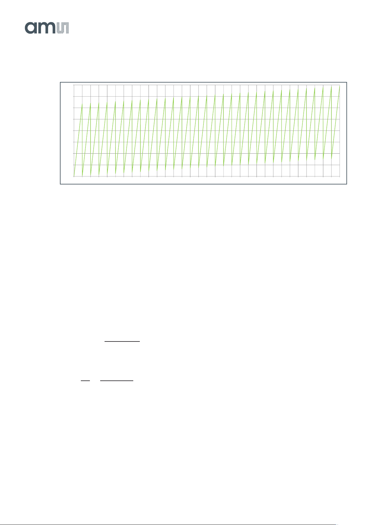
The pattern consists of increasing pixel values per column per channel. The first column of each (top
and bottom) channel, offsets with 1 compared to the previous channel. So channels 1/33 will contain
0, 1, 2 … 126, 127 and channels 2/34 contain 1, 2, 3 … 127, 128 and channels 32/64 contain 31, 32,
33 … 157, 158 and so on.
To have the same test pattern in 8b as in 10b and 12b, the digital gain has to be set to 16. Set it back
to 6 when taking normal images again.
Figure 84:
Test Pattern Setting
Reg. Name
Address
Bits
Default
Description
Test
122
[1:0]
0
0: Off
3: On
Figure 85:
Test Pattern Image
Document Feedback
CMV12000
Functional Description
Datasheet • PUBLIC
DS000603 • v6-00 • 2023-Sep-22
84 │ 62
Figure 86:
Test Pattern Data
7.6.5 Temperature Sensor
A 16-bit digital temperature sensor is included in the image sensor and can be controlled by the SPI-
interface. An input clock at pin CLK_IN must be applied to use the temperature sensor. The on-chip
temperature can be calculated by reading out the Temp_sensor register.
The value in the temperature sensor register is dependent on the CLK_IN frequency. The value has
an offset (so at 0 °C the value in this register is not 0) and a slope (DN/°C). Both are input clock
dependent. For example, if you read out a value of 1000DN at 40 MHz, you will read a value of 500DN
at 20 MHz at the same temperature.
The offset and slope values will vary between devices. The typical offset and slope values are:
Equation 6:
Equation 7:
As the offset value varies between devices, at least a 1-point calibration per device should be done at
a known temperature to compensate this offset. As the slope variation is and has less of an influence
on the accuracy, a 2-point calibration is only needed if higher accuracy of the temperature is needed.
Below is an example of two devices (CLK_IN = 60 MHz) register values at different temperatures. The
offset and slope vary about 300DN and 0.5DN/°C between each other. You can clearly see that not
calibrating for the offset difference (so using 1600DN) will result in a very large error while using the
typical 7DN/°C will yield only small inaccuracy.
0
20
40
60
80
100
120
140
160
0 128 256 384 512 640 768 896 1024 1152 1280 1408 1536 1664 1792 1920 2048 2176 2304 2432 2560 2688 2816 2944 3072 3200 3328 3456 3584 3712 3840 3968 4096
Output [DN]
Column number