CMV12000_DS000603_6-00.pdf - 第80页
Document Feedback CMV12000 Package Drawings & Markings Datasheet • PUBLIC DS000603 • v6 - 00 • 2023 -Sep- 22 84 │ 79 Figure 102 : 237p µPGA Package Assembly Outline Drawing (1) All dimensions are in mm (2) Rotation o…
Document Feedback
CMV12000
Package Drawings & Markings
Datasheet • PUBLIC
DS000603 • v6-00 • 2023-Sep-22
84 │ 78
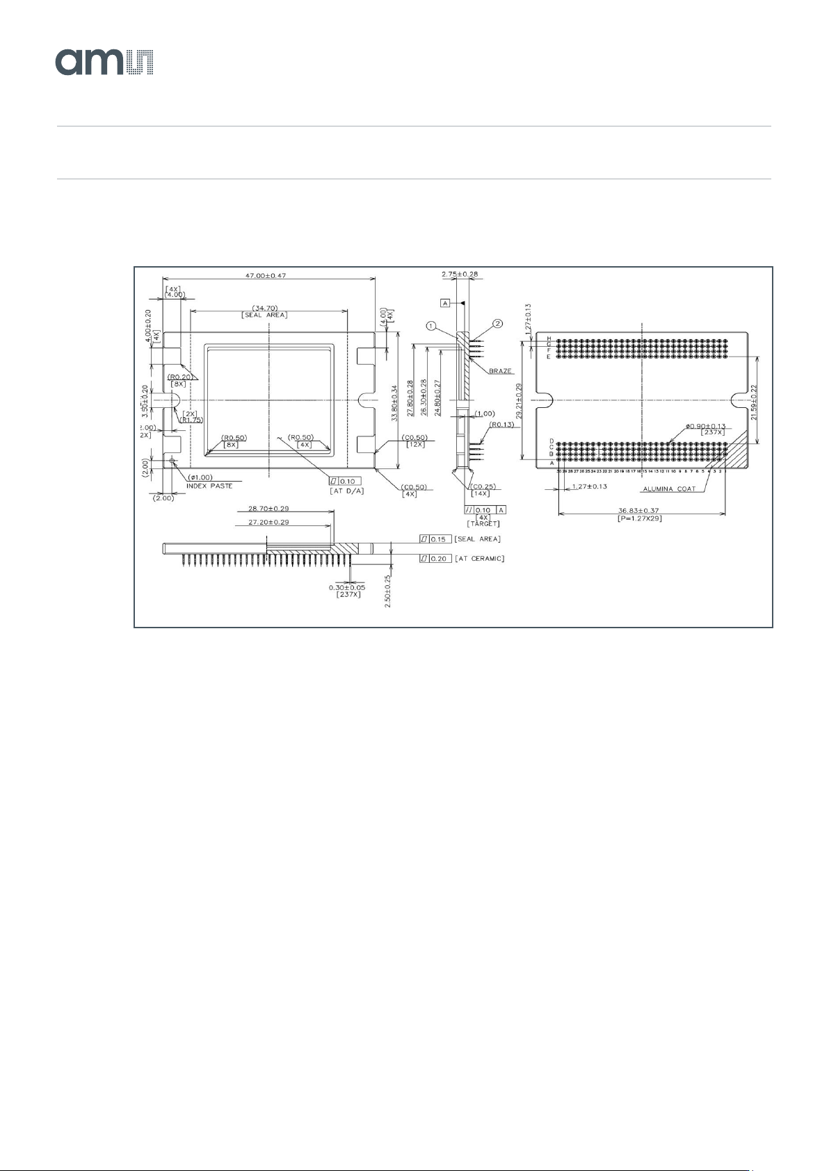
10 Package Drawings & Markings
Figure 101:
237p µPGA Package Outline Drawing
(1) All dimensions are in mm
(2) Pin material: Kovar
(3) Pin plating: Au 1.5 µm min. over Ni 2.0 µm min.
(4) Ceramic material: Alumina (Al
2
O
3
)
(5) Ceramic properties: Thermal Conductivity = 18 W/m.K; Young’s mod = 280GPa; CTE = 7.6×10
-6
/K
Document Feedback
CMV12000
Package Drawings & Markings
Datasheet • PUBLIC
DS000603 • v6-00 • 2023-Sep-22
84 │ 79
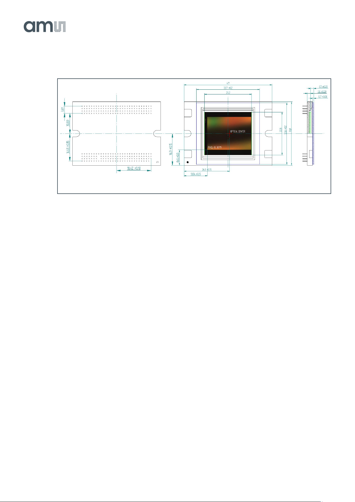
Figure 102:
237p µPGA Package Assembly Outline Drawing
(1) All dimensions are in mm
(2) Rotation of the die referenced to the package outside: ±0.5 degrees
(3) Tilt of the die referenced to the die attach area (cavity bottom): ±0.15 degrees
(4) Distance top of pixel array to top of cover glass: 1.7 ±0.20 mm
(5) Cover glass: plain D263 with AR coating on both sides. When a color filter is used, an IR-cutoff filter should be placed in
the optical path for color accuracy.