CMV12000_DS000603_6-00.pdf - 第30页
Document Feedback CMV12000 Functional Description Datasheet • PUBLIC DS000603 • v6 - 00 • 2023 -Sep- 22 84 │ 29 7.3.2 Low-Level Readout Format The data is transferred LSB first, with the transfer of bit D[0] during the h…

Document Feedback
CMV12000
Functional Description
Datasheet • PUBLIC
DS000603 • v6-00 • 2023-Sep-22
84 │ 28
Figure 24:
External Exposure Extension
7.3 Sensor Readout Format
7.3.1 LVDS Outputs
The CMV12000 has LVDS (low voltage differential signaling) outputs to transport the image data to
the surrounding system. Next to 64 data channels, the sensor also has two other LVDS channels for
control and synchronization of the image data. In total, the sensor has 66 LVDS output pairs (2 pins
for each LVDS channel):
● 64 data channels
● 1 control channel
● 1 clock channel
This means that a total of 132 pins of the CMV12000 are used for the LVDS outputs (128 for data + 2
for LVDS clock + 2 for control channel). See the pin list in Figure 4 for the exact pin numbers of the
LVDS outputs.
The 64 data channels are used to transfer the 12-bit, 10-bit or 8-bit pixel data from the sensor to the
receiver in the surrounding system. The 32 bottom channels use pins OUT1_N/P to OUT32_N/P and
the top channels use pins OUT33_P/N to OUT64_P/N.
The output clock channel transports a clock, synchronous to the data on the other LVDS channels.
This clock can be used at the receiving end to sample the data. This clock is DDR, which means that
the frequency will be half of the output data rate. When 600 Mbit/s output data rate is used, the LVDS
output clock will be 300 MHz (half of input clock).
The data on the control channel contains status information on the validity of the data on the data
channels. Information on the control channel is grouped in 8-bit, 10-bit or 12-bit words that are
transferred synchronous to the 64 data channels.
FOT
READOUT
INTE
FOT READOUT
T_EXP
Frame_REQ
extended INTEINTE
delayed
Current Frame
Next Frame
Document Feedback
CMV12000
Functional Description
Datasheet • PUBLIC
DS000603 • v6-00 • 2023-Sep-22
84 │ 29
7.3.2 Low-Level Readout Format
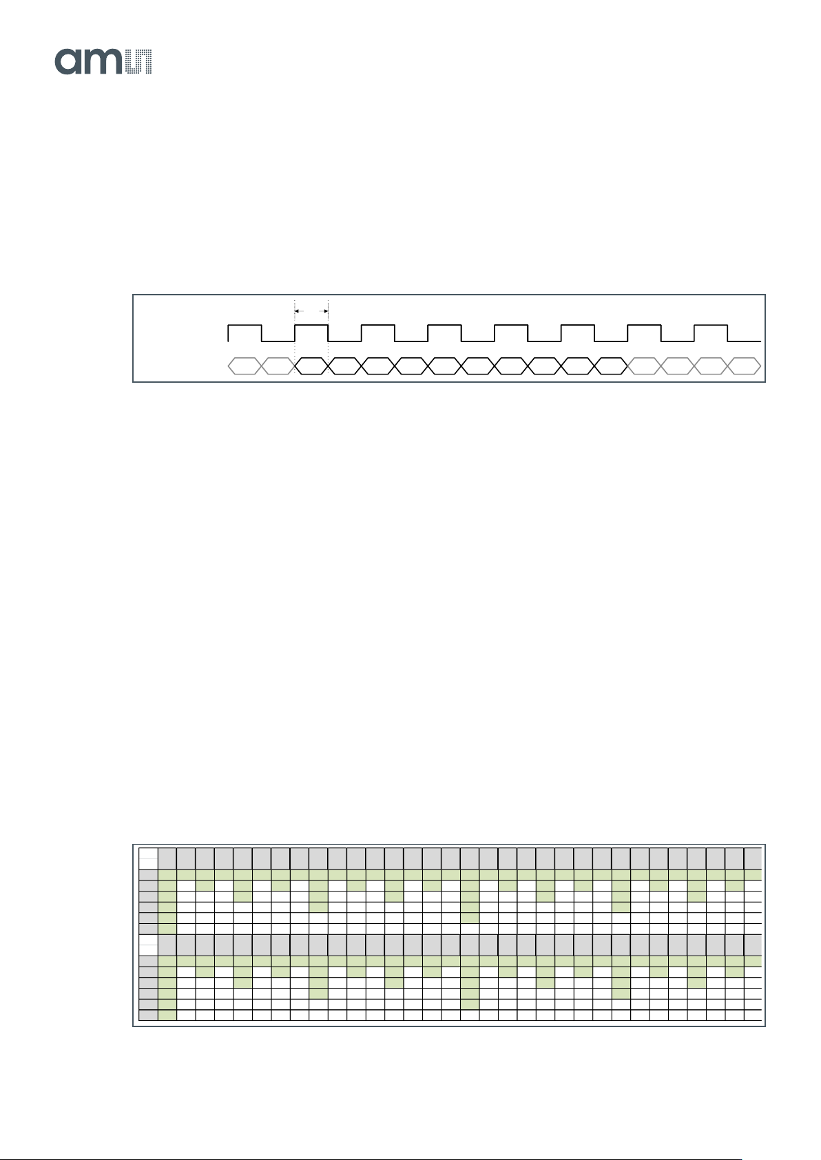
The data is transferred LSB first, with the transfer of bit D[0] during the high phase of the DDR output
clock. An example of 10b mode is shown below for the P-channel of one LVDS channel. T1 is the
period of the input clock (600 MHz input clock = 300 MHz output clock).
Figure 25:
10b Pixel Data on an LVDS Channel
7.3.3 Pixel Readout Format
The read-out of image data is grouped in bursts of 128 pixels per channel (2 rows at the same time via
top and bottom outputs). Each pixel is 8, 10 or 12 bits wide. For details on pixel remapping and pixel
vs. channel location please see section 7.3.4. An overhead time exists between two bursts of 128
pixels. This overhead time has the length of one pixel read-out (i.e. the length of 8, 10 or 12 bits at the
selected data rate).
Please note that depending on the bit mode (8-bit, 10-bit or 12-bit) and read-out mode (subsampling,
binning…), the actual timing of the image data may differ from one mode to another. The sections
below show the relative location of the pixel data only.
The sensor is designed to be used with both sides (bottom and top) simultaneously. There is a “one
side mode” where only one side (bottom) can be used to read out data, but binning and subsampling
in X and Y direction are not supported in this mode.
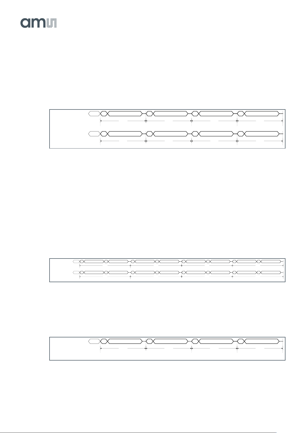
The sensor is able to send all pixel data over fewer channels. The overview of which outputs are used
when multiplexing to fewer outputs is shown below.
Figure 26:
Channel Muxing Overview
D(8) D(9) D(0) D(1) D(2) D(3) D(4) D(5) D(6) D(7) D(8) D(9) D(0) D(1) D(2) D(3)
T1
LVDS_CLOCK
_OUT
DATA_OUT
OUT OUT OUT OUT OUT OUT OUT OUT OUT OUT OUT OUT OUT OUT OUT OUT OUT OUT OUT OUT OUT OUT OUT OUT OUT OUT OUT OUT OUT OUT OUT OUT
1 2 3 4 5 6 7 8 9 10 11 12 13 14 15 16 17 18 19 20 21 22 23 24 25 26 27 28 29 30 31 32
32 x x x x x x x x x x x x x x x x x x x x x x x x x x x x x x x x
16 x x x x x x x x x x x x x x x x
8 x x x x x x x x
4 x x x x
2 x x
1 x
OUT OUT OUT OUT OUT OUT OUT OUT OUT OUT OUT OUT OUT OUT OUT OUT OUT OUT OUT OUT OUT OUT OUT OUT OUT OUT OUT OUT OUT OUT OUT OUT
33 34 35 36 37 38 39 40 41 42 43 44 45 46 47 48 49 50 51 52 53 54 55 56 57 58 59 60 61 62 63 64
32 x x x x x x x x x x x x x x x x x x x x x x x x x x x x x x x x
16 x x x x x x x x x x x x x x x x
8 x x x x x x x x
4 x x x x
2 x x
1 x
Document Feedback
CMV12000
Functional Description
Datasheet • PUBLIC
DS000603 • v6-00 • 2023-Sep-22
84 │ 30
By default, all 64 data output channels are used to transmit the image data. This means that two entire
rows of image data are transferred (one using the top outputs and one using the bottom outputs) in
one slot of 128 pixel periods (64 × 128 = 8192). Next figure shows the timing for the top and bottom
LVDS channels. The bottom channels read out the odd rows (start at 1) and the top channels read out
the even rows.
Figure 27:
Data Output Timing with 64 (2 × 32) Channels
Only when 64 data outputs, running at 600 Mbit/s in 10b mode are used, the frame rate of 300 fps can
be achieved.
Using less output channels, this can be programmed with register 81. In this multiplexed mode, the
read-out of one row takes N × 128 periods (but two rows will be sent out at the same time). N = 1, 2, 3
… for 32, 16, 8 … channels per side. Each block of 128 pixels (=DVAL) is separated by one OH, while
each row of pixels (=LVAL) is separated by a longer OH (depending on the number of outputs and
sides, subsampling and binning).
Next figure shows the timing when multiplexing to 16 channels on each side.
Figure 28:
Data Output Timing with 2 × 16 Channels
When using the ‘one side mode’, each row is readout by the bottom outputs following the pattern in
the figure below.
Figure 29:
One Side Readout Mode with 32 (1 × 32) Channels
IDLE OH 128 OHDATA_OUT_BOTTOM 128 OH 128
Row 1 Row3 Row5
OH 128
Row7
IDLE OH 128 OHDATA_OUT_TOP 128 OH 128
Row2 Row4 Row6
2x32CH
OH 128
Row8
IDLE OH 128 OH
DATA_OUT_TOP
128 OH 128
Row2 Row4
OH 128 OH 128 OH 128
Row6
2x16CH
OH 128 OH 128
Row8
IDLE OH 128 OHDATA_OUT_BOTTOM 128 OH 128
Row 1 Row3
OH 128 OH 128 OH 128
Row5
OH 128 OH 128
Row7
IDLE OH 128 OHDATA_OUT_BOTTOM 128 OH 128
Row 1 Row 2 Row 4
1x32CH
OH 128
Row 3