CMV12000_DS000603_6-00.pdf - 第81页
Document Feedback CMV12000 Packing Information Datasheet • PUBLIC DS000603 • v6 - 00 • 2023 -Sep- 22 84 │ 80 11 Packing Information Devices are shipped in a 3×6 matrix 33.8× 47 µPGA JEDEC tray.
Document Feedback
CMV12000
Package Drawings & Markings
Datasheet • PUBLIC
DS000603 • v6-00 • 2023-Sep-22
84 │ 79
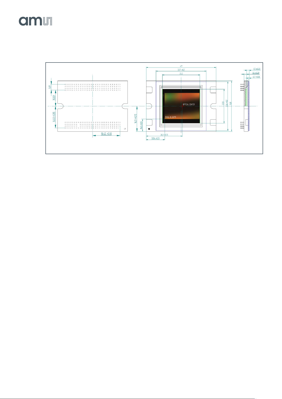
Figure 102:
237p µPGA Package Assembly Outline Drawing
(1) All dimensions are in mm
(2) Rotation of the die referenced to the package outside: ±0.5 degrees
(3) Tilt of the die referenced to the die attach area (cavity bottom): ±0.15 degrees
(4) Distance top of pixel array to top of cover glass: 1.7 ±0.20 mm
(5) Cover glass: plain D263 with AR coating on both sides. When a color filter is used, an IR-cutoff filter should be placed in
the optical path for color accuracy.

Document Feedback
CMV12000
Soldering & Storage Information
Datasheet • PUBLIC
DS000603 • v6-00 • 2023-Sep-22
84 │ 81
12 Soldering & Storage Information
12.1 Soldering
CMV12000 is not shipped in a moisture barrier package. When reflow soldering, a dry bake needs to
be performed upfront! The CMV12000 device has passed MSL3 testing. Figure 103 shows the
maximum recommended thermal profile for a reflow soldering system (following Standard J-STD-020).
If the temperature/time profile exceeds these recommendations, damage to the image sensor can
occur.
Attention
1. Image sensors with color filter arrays (CFA) and micro lenses are especially sensitive to high
temperatures. Prolonged heating at elevated temperatures may result in deterioration of the
optical performance of the sensor.
2. A socket (see 9.2) is the safest way to avoid any thermal stress. When not using a socket, to
avoid heating up the device we recommend to use manual hand soldering. Wave soldering
can be used with precautions (see below). Reflow soldering is not recommended.
Manual soldering: Use partial heating method and use a soldering iron with temperature control. The
soldering iron tip temperature is not to exceed 350 °C with a 270 °C maximum pin temperature. Touch
for a 2 seconds maximum duration per pin. Avoid touching and global heating of the ceramic package
during soldering. Failure to do so may alter device performance and reliability.
Wave soldering: Wave solder dipping can cause damage to the glass and harm the imaging capability
of the device. Avoid the solder to come in contact with the glass or ceramic body.