CMV12000_DS000603_6-00.pdf - 第32页
Document Feedback CMV12000 Functional Description Datasheet • PUBLIC DS000603 • v6 - 00 • 2023 -Sep- 22 84 │ 31 7.3.4 Pixel Remapping Depending on the number of output channels, the pixels are located at different cha nn…
Document Feedback
CMV12000
Functional Description
Datasheet • PUBLIC
DS000603 • v6-00 • 2023-Sep-22
84 │ 30
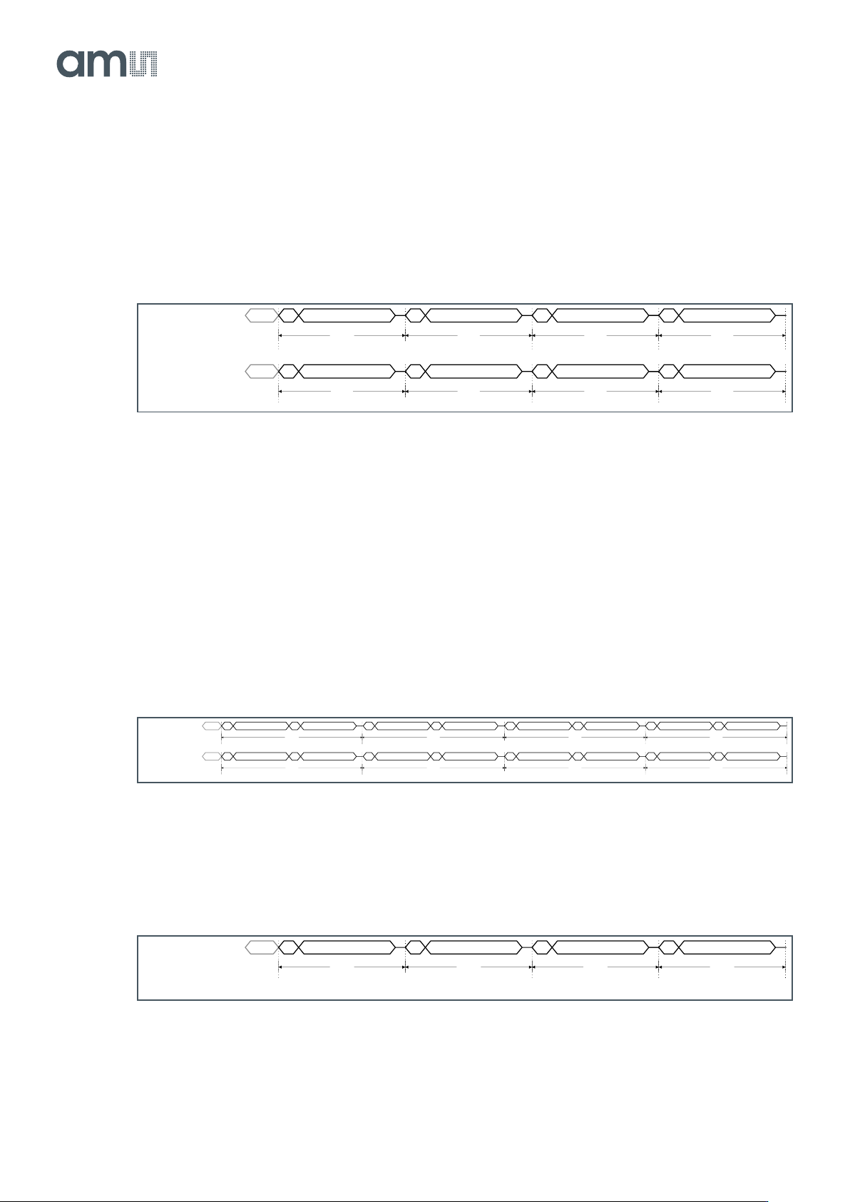
By default, all 64 data output channels are used to transmit the image data. This means that two entire
rows of image data are transferred (one using the top outputs and one using the bottom outputs) in
one slot of 128 pixel periods (64 × 128 = 8192). Next figure shows the timing for the top and bottom
LVDS channels. The bottom channels read out the odd rows (start at 1) and the top channels read out
the even rows.
Figure 27:
Data Output Timing with 64 (2 × 32) Channels
Only when 64 data outputs, running at 600 Mbit/s in 10b mode are used, the frame rate of 300 fps can
be achieved.
Using less output channels, this can be programmed with register 81. In this multiplexed mode, the
read-out of one row takes N × 128 periods (but two rows will be sent out at the same time). N = 1, 2, 3
… for 32, 16, 8 … channels per side. Each block of 128 pixels (=DVAL) is separated by one OH, while
each row of pixels (=LVAL) is separated by a longer OH (depending on the number of outputs and
sides, subsampling and binning).
Next figure shows the timing when multiplexing to 16 channels on each side.
Figure 28:
Data Output Timing with 2 × 16 Channels
When using the ‘one side mode’, each row is readout by the bottom outputs following the pattern in
the figure below.
Figure 29:
One Side Readout Mode with 32 (1 × 32) Channels
IDLE OH 128 OHDATA_OUT_BOTTOM 128 OH 128
Row 1 Row3 Row5
OH 128
Row7
IDLE OH 128 OHDATA_OUT_TOP 128 OH 128
Row2 Row4 Row6
2x32CH
OH 128
Row8
IDLE OH 128 OH
DATA_OUT_TOP
128 OH 128
Row2 Row4
OH 128 OH 128 OH 128
Row6
2x16CH
OH 128 OH 128
Row8
IDLE OH 128 OHDATA_OUT_BOTTOM 128 OH 128
Row 1 Row3
OH 128 OH 128 OH 128
Row5
OH 128 OH 128
Row7
IDLE OH 128 OHDATA_OUT_BOTTOM 128 OH 128
Row 1 Row 2 Row 4
1x32CH
OH 128
Row 3
Document Feedback
CMV12000
Functional Description
Datasheet • PUBLIC
DS000603 • v6-00 • 2023-Sep-22
84 │ 31
7.3.4 Pixel Remapping
Depending on the number of output channels, the pixels are located at different channels and are read
out at a different moment in time. With the details from the next sections, the end user is able to remap
the pixels on the outputs to their correct image array location.
Two Sided Readout Mode
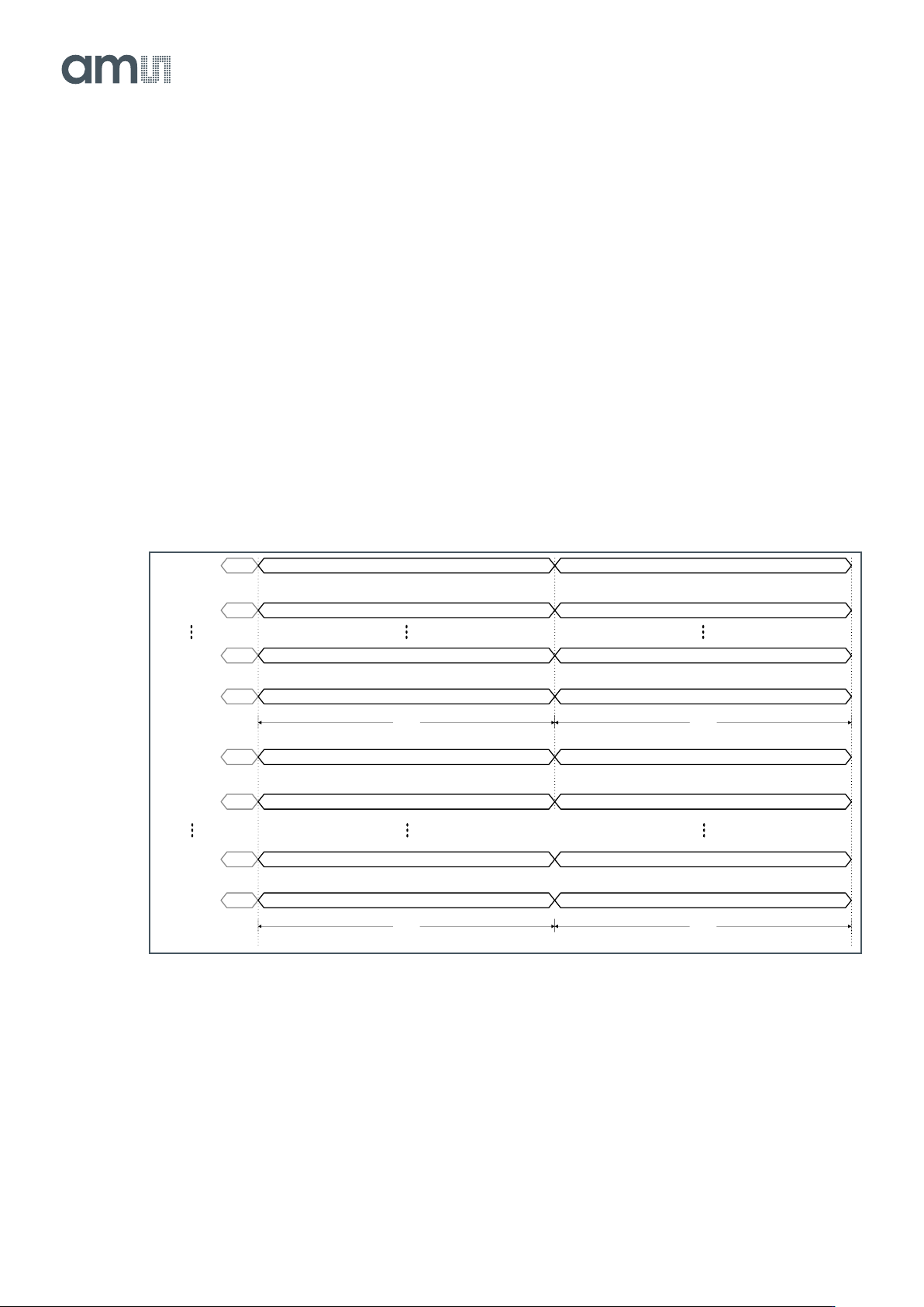
Below are two examples of the pixel mapping when using 2 × 32 channels and 2 × 16 channels. It will
be similar for less channels.
64 bursts (2 × 32) of 128 pixels happen in parallel on the data outputs. This means that two complete
rows are read out in one burst; the odd rows via the bottom channels, the even rows via the top
channels. The amount of rows that will be read out depends on the value in the corresponding
register. By default there are 3072 rows read out.
Figure 30:
Pixel Mapping Using 2 x 32 Channels
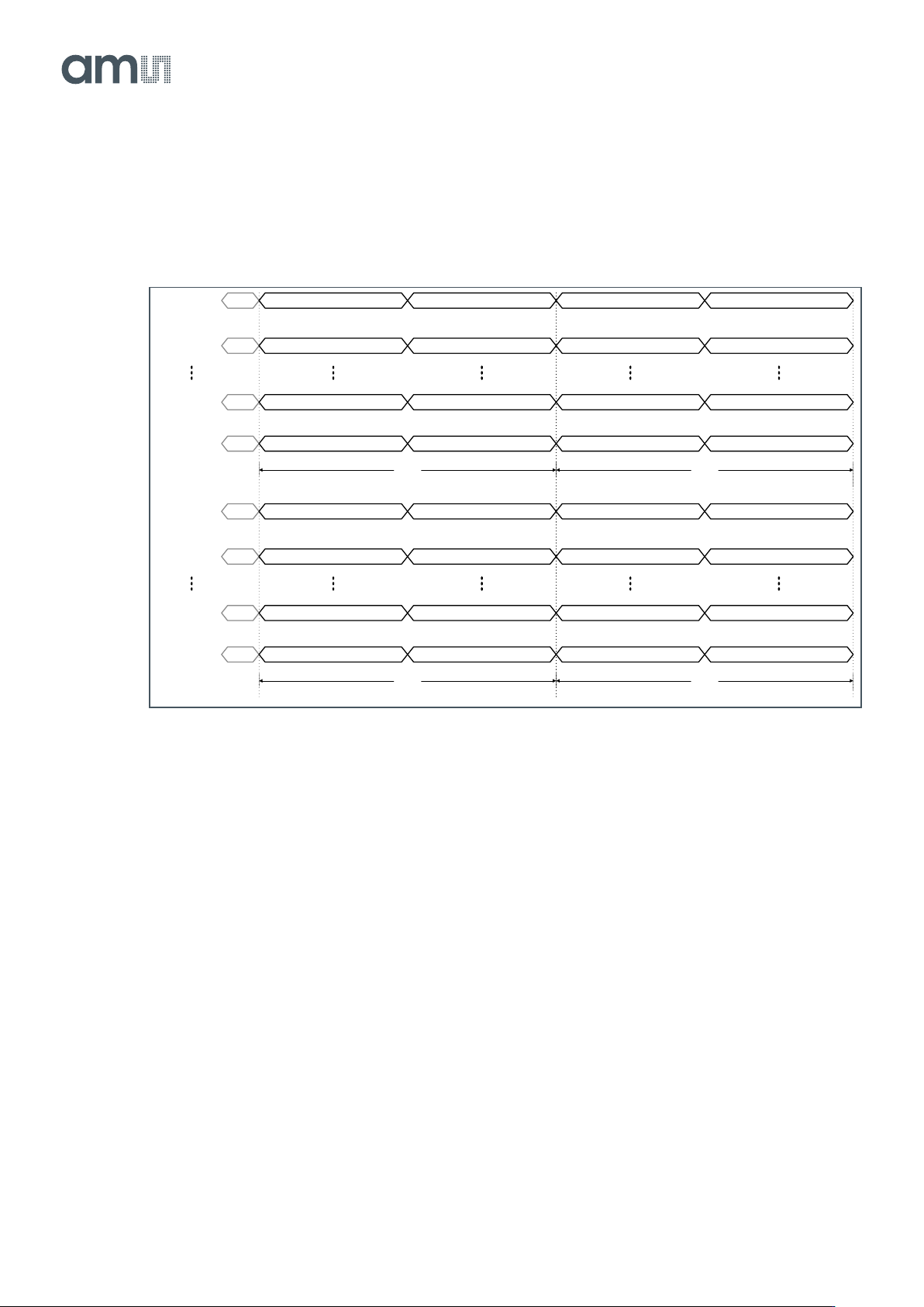
When 2 × 16 output mode is used, the pixel data is placed on the outputs as detailed in the figure
below. 16 bursts of 128 pixels happen in parallel on the data outputs on both sides simultaneous (16
on the top and 16 on the bottom outputs); the odd rows via the bottom channels, the even rows via the
top channels. This means that one complete row one each side is read out in two burst (so effectively
two rows are read-out in two bursts).
The time needed to read out two rows is doubled compared to when 64 outputs are used. The even
LVDS channels are not being used in this case, so they can be turned off by setting the correct bits in
IDLE Pixel 0 to 127Channel 1
IDLEChannel 2
Row 1
Pixel 128 to 255
IDLEChannel 31 Pixel 3840 to 3967
IDLEChannel 32 Pixel 3968 to 4095
Pixel 0 to 127
Row 3
Pixel 128 to 255
Pixel 3840 to 3967
Pixel 3968 to 4095
IDLE Pixel 0 to 127Channel 33
IDLEChannel 34
Row 2
Pixel 128 to 255
IDLEChannel 63 Pixel 3840 to 3967
IDLE
Channel 64
Pixel 3968 to 4095
Pixel 0 to 127
Row 4
Pixel 128 to 255
Pixel 3840 to 3967
Pixel 3968 to 4095
2x32CH
Document Feedback
CMV12000
Functional Description
Datasheet • PUBLIC
DS000603 • v6-00 • 2023-Sep-22
84 │ 32
the register with addresses 92-93. Turning off these channels will reduce the power consumption of
the chip. The amount of rows that will be read out depends on the value in the corresponding register.
By default there are 3072 rows being read out.
Figure 31:
Pixel Mapping Using 2 x 16 Channels
One Sided Readout Mode
When only one side is used, the pixel data is placed on the outputs as detailed in the figure below
(example of 1 × 32 and 1 × 16). N bursts of 128 pixels happen in parallel on the data outputs. This
means that one complete row is read out in one burst. The rows will be read out following the pattern:
row 1, row 2, row 4, row 3, row 5, row 6, row 8, row 7… So every 3
rd
and 4
th
row are switched.
The time needed to read out two rows is doubled compared to when 64 outputs are used. The top
LVDS channels are not being used in this mode, so they can be turned off by setting the correct bits in
the register with addresses 92-93. Turning off these channels will reduce the power consumption of
the chip. The amount of rows that will be read out depends on the value in the corresponding register.
By default there are 3072 rows read out.
IDLE Pixel 0 to 127Channel 1
IDLEChannel 3
Row 1
Pixel 256 to 383
IDLEChannel 29 Pixel 3584 to 3711
IDLEChannel 31 Pixel 3840 to 3967
Pixel 128 to 255
Pixel 384 to 511
Pixel 3712 to 3839
Pixel 3968 to 4095
IDLE Pixel 0 to 127Channel 33
IDLEChannel 35
Row 2
Pixel 256 to 383
IDLEChannel 61 Pixel 3584 to 3711
IDLEChannel 63 Pixel 3840 to 3967
Pixel 128 to 255
Pixel 384 to 511
Pixel 3712 to 3839
Pixel 3968 to 4095
2x16CH
Pixel 0 to 127
Row 3
Pixel 256 to 383
Pixel 3584 to 3711
Pixel 3840 to 3967
Pixel 128 to 255
Pixel 384 to 511
Pixel 3712 to 3839
Pixel 3968 to 4095
Pixel 0 to 127
Row 4
Pixel 256 to 383
Pixel 3584 to 3711
Pixel 3840 to 3967
Pixel 128 to 255
Pixel 384 to 511
Pixel 3712 to 3839
Pixel 3968 to 4095